ZHCSFJ6B August 2016 – March 2022 UCD9090A
PRODUCTION DATA
- 1 特性
- 2 应用
- 3 说明
- 4 Revision History
- 5 Pin Configuration and Functions
- 6 Specifications
-
7 Detailed Description
- 7.1 Overview
- 7.2 Functional Block Diagram
- 7.3 Feature Description
- 7.4
Device Functional Modes
- 7.4.1 Power Supply Sequencing
- 7.4.2 Pin-Selected Rail States
- 7.4.3 Monitoring
- 7.4.4 Fault Responses and Alert Processing
- 7.4.5 Shut Down All Rails and Sequence On (Resequence)
- 7.4.6 GPIOs
- 7.4.7 GPO Control
- 7.4.8 GPO Dependencies
- 7.4.9 GPI Special Functions
- 7.4.10 Power Supply Enables
- 7.4.11 Cascading Multiple Devices
- 7.4.12 PWM Outputs
- 7.4.13 Programmable Multiphase PWMs
- 7.4.14 Margining
- 7.4.15 Run Time Clock
- 7.4.16 System Reset Signal
- 7.4.17 Watch Dog Timer
- 7.4.18 Data and Error Logging to Flash Memory
- 7.4.19 Brownout Function
- 7.4.20 PMBus Address Selection
- 7.4.21 Device Reset
- 7.4.22 JTAG Interface
- 7.4.23 Internal Fault Management and Memory Error Correction (ECC)
- 7.5 Programming
- 8 Application and Implementation
- 9 Power Supply Recommendations
- 10Layout
- 11Device and Documentation Support
- 12Mechanical, Packaging, and Orderable Information
封装选项
请参考 PDF 数据表获取器件具体的封装图。
机械数据 (封装 | 引脚)
- RGZ|48
散热焊盘机械数据 (封装 | 引脚)
- RGZ|48
订购信息
7.4.8 GPO Dependencies
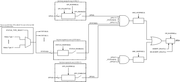
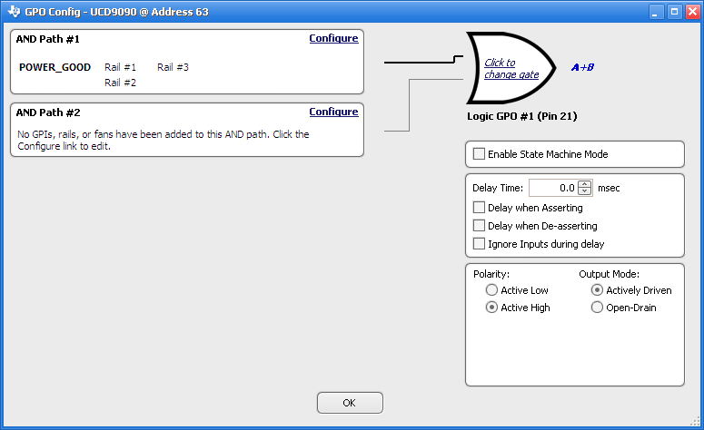
GPIOs can be configured as outputs that are based on Boolean combinations of up to two ANDs all ORed together (Figure 7-13). Inputs to the logic blocks can include the first 8 defined GPOs, GPIs and rail-status flags. One rail status type is selectable as an input for each AND gate in a Boolean block. For a selected rail status, the status flags of all active rails can be included as inputs to the AND gate. _LATCH rail-status types stay asserted until cleared by a MFR PMBus command or by a specially configured GPI pin. The different rail-status types are shown in Table 7-5. See the UCD90xxx Sequencer and System Health Controller PMBus Command Reference for complete definitions of rail-status types. The GPO response can be configured to have a delayed assertion or deassertion. The first 8 GPOs can be chosen as Rail Sequence on/off Dependency. The logic state of the GPO instead of actual pin output is used as dependency condition.
 Figure 7-13 Boolean Logic Combinations
 Figure 7-14 Fusion Boolean Logic Builder
| Rail-Status Types | ||
|---|---|---|
| POWER_GOOD | IOUT_UC_FAULT | TOFF_MAX_WARN_LATCH |
| MARGIN_EN | TEMP_OT_FAULT | SEQ_ON_TIMEOUT_LATCH |
| MRG_LOW_nHIGH | TEMP_OT_WARN | SEQ_OFF_TIMEOUT_LATCH |
| VOUT_OV_FAULT | SEQ_ON_TIMEOUT | SYSTEM_WATCHDOG_TIMEOUT_LATCH |
| VOUT_OV_WARN | SEQ_OFF_TIMEOUT | IOUT_OC_FAULT_LATCH |
| VOUT_UV_WARN | SYSTEM_WATCHDOG_TIMEOUT | IOUT_OC_WARN_LATCH |
| VOUT_UV_FAULT | VOUT_OV_FAULT_LATCH | IOUT_UC_FAULT_LATCH |
| TON_MAX_FAULT | VOUT_OV_WARN_LATCH | TEMP_OT_FAULT_LATCH |
| TOFF_MAX_WARN | VOUT_UV_WARN_LATCH | TEMP_OT_WARN_LATCH |
| IOUT_OC_FAULT | VOUT_UV_FAULT_LATCH | |
| IOUT_OC_WARN | TON_MAX_FAULT_LATCH | |
When GPO is set to POWER_GOOD, this POWER_GOOD state is based on the actual voltage measurement on the monitor pins assigned to those rails. For a rail that does not have a monitor pin, or have a monitor pin but without voltage monitoring, its POWER_GOOD state is used by sequencing purpose only, and is not be used by the GPO logic evaluation.