SCBS809G December 2005 – September 2017 UCC2895-EP
PRODUCTION DATA.
5 Specifications
5.1 Absolute Maximum Ratings(1)(2)
over operating free-air temperature range (unless otherwise noted)| MIN | MAX | UNIT | |||
|---|---|---|---|---|---|
| Supply voltage | IDD < 10 mA | 17 | V | ||
| Supply current | 30 | mA | |||
| REF current | 15 | mA | |||
| OUT current | 100 | mA | |||
| Analog inputs | EAP, EAN, EAOUT, RAMP, SYNC, ADS, CS, SS/DISB | –0.3 | REF + 0.3 | V | |
| Drive outputs | OUTA, OUTB, OUTC, OUTD | –0.3 | to VCC + 0.3 | V | |
| Power dissipation (at TA = 25°C) |
N package | 1 | W | ||
| DW package | 650 | mW | |||
| Storage temperature, Tstg | –65 | 150 | °C | ||
| Junction temperature, TJ | –55 | 150 | °C | ||
| Lead temperature | Soldering, 10 s | 300 | °C | ||
(1) Stresses beyond those listed under Absolute Maximum Ratings may cause permanent damage to the device. These are stress ratings only, which do not imply functional operation of the device at these or any other conditions beyond those indicated under Recommended Operating Conditions. Exposure to absolute-maximum-rated conditions for extended periods may affect device reliability.
(2) Currents are positive into and negative out of the specified terminal.
5.2 ESD Ratings
| VALUE | UNIT | |||
|---|---|---|---|---|
| V(ESD) | Electrostatic discharge | Human-body model (HBM), per ANSI/ESDA/JEDEC JS-001(1) | ±800 | V |
| Charged-device model (CDM), per JEDEC specification JESD22-C101(2) | ±2000 | |||
(1) JEDEC document JEP155 states that 500-V HBM allows safe manufacturing with a standard ESD control process.
(2) JEDEC document JEP157 states that 250-V CDM allows safe manufacturing with a standard ESD control process.
5.3 Recommended Operating Conditions(1)
over operating free-air temperature range (unless otherwise noted)| MIN | NOM | MAX | UNIT | ||
|---|---|---|---|---|---|
| VDD | Supply voltage | 10 | 16.5 | V | |
| CVDD | Supply voltage bypass capacitor(2) | 10 x CREF | µF | ||
| CREF | Reference bypass capacitor(3) | 0.1 | 4.7 | µF | |
| CT | Timing capacitor (for 500-KHz switching frequency) | 200 | pF | ||
| RT | Timing resistor (for 500-KHz switching frequency) | 82 | |||
| RDEL_AB
RDEL_CD |
Delay resistor | 2.5 | 40 | kΩ | |
| TJ | Operating junction temperature(4) | –55 | 125 | °C | |
(1) It is recommended that there be a single point grounded between GND and PGND directly under the device. There should be a seperate ground plane associated with the GND pin and all components associated with pins 1 through 12 plus 19 and 20 be located over this ground plane. Any connections associated with these pins to ground should be connected to this ground plane.
(2) The VDD capacitor should be a low ESR, ESL ceramic capacitor located directly across the VDD and PGND pins. A larger bulk capacitor should be located as physically close as possible to the VDD pins.
(3) The VREF capacitor should be a low ESR, ESL ceramic capacitor located directly across the REF and GND pins. If a larger capacitor is desired for the VREF then it should be located near the VREF capacitor and connected to the VREF pin with a resistor of 51 Ω or greater. The bulk capacitor on VDD must be a factor of 10 greater than the total VREF capacitance.
(4) It is not recommended that the device operate under conditions beyond those specified in this table for extended periods of time.
5.4 Thermal Information
| THERMAL METRIC(1) | UCC2895-EP | UNIT | |
|---|---|---|---|
| DW (SOIC) | |||
| 20 PINS | |||
| RθJA | Junction-to-ambient thermal resistance | 59.9 | °C/W |
| RθJC(top) | Junction-to-case (top) thermal resistance | 28.3 | °C/W |
| RθJB | Junction-to-board thermal resistance | 27.8 | °C/W |
| ψJT | Junction-to-top characterization parameter | 7.4 | °C/W |
| ψJB | Junction-to-board characterization parameter | 27.4 | °C/W |
(1) For more information about traditional and new thermal metrics, see the Semiconductor and IC Package Thermal Metrics application report.
5.5 Electrical Characteristics
VDD = 12 V, RT = 82 kΩ, CT = 220 pF, RDELAB = 10 kΩ, RDELCD = 10 kΩ, CREF = 0.1 μF, CVDD = 1 μF, No load at outputs,TA = TJ, TA = –55°C to 125°C (unless otherwise noted)
| PARAMETER | TEST CONDITIONS | MIN | TYP | MAX | UNIT |
|---|---|---|---|---|---|
| UVLO | |||||
| Start threshold | 10.2 | 11 | 11.8 | V | |
| Stop threshold | 8.2 | 9 | 9.8 | V | |
| Hysteresis | 1 | 2 | 3 | V | |
| SUPPLY CURRENT | |||||
| Start-up current | VDD = 8 V | 150 | 250 | μA | |
| IDD active | 5 | 6 | mA | ||
| VCC clamp voltage | IDD = 10 mA | 16.5 | 17.5 | 18.5 | V |
| VOLTAGE REFERENCE | |||||
| Output voltage | TJ = 25°C | 4.94 | 5 | 5.06 | V |
| 10 V < VDD < 17.5 V, 0 mA < IREF < 5 mA | 4.85 | 5 | 5.15 | ||
| Short-circuit current | REF = 0 V, TJ = 25°C | 10 | 20 | mA | |
| ERROR AMPLIFIER | |||||
| Common-mode input voltage | –0.1 | 3.6 | V | ||
| Offset voltage | –7 | 7 | mV | ||
| Input bias current (EAP, EAN) | –1 | 1 | μA | ||
| EAOUT VOH | EAP – EAN = 500 mV, IEAOUT = –0.5 mA | 4 | 4.5 | 5 | V |
| EAOUT VOL | EAP – EAN = 500 mV, IEAOUT = 0.5 mA | 0 | 0.2 | 0.4 | V |
| EAOUT source current | EAP – EAN = 500 mV, EAOUT = 2.5 V | 1 | 1.5 | mA | |
| EAOUT sink current | EAP – EAN = –500 mV, EAOUT = 2.5 V | 2.5 | 4.5 | mA | |
| Open-loop DC gain | 75 | 85 | dB | ||
| Unity gain bandwidth(1) | 5 | 7 | MHz | ||
| Slew rate | EAN from 1 V to 0 V, EAP = 500 mV, EAOUT from 0.5 V to 3 V(1) |
1.5 | 2.2 | V/μs | |
| No-load comparator turn-off threshold | 0.45 | 0.5 | 0.55 | V | |
| No-load comparator turn-on threshold | 0.55 | 0.6 | 0.69 | V | |
| No-load comparator hysteresis | 0.035 | 0.1 | 0.165 | V | |
| OSCILLATOR | |||||
| Frequency | TJ = 25°C | 473 | 500 | 527 | kHz |
| Total variation | Line, Temperature(1) | 2.5% | 5% | ||
| SYNC VIH | 2.05 | 2.1 | 2.32 | V | |
| SYNC VIL | 1.85 | 1.9 | 1.95 | V | |
| SYNC VOH | ISYNC = –400 μA, CT = 2.6 V | 4.1 | 4.5 | 5 | V |
| SYNC VOL | ISYNC = 100 μA, CT = 0 V | 0 | 0.5 | 1 | V |
| SYNC output pulse width | SYNC load = 3.9 kΩ and 30 pF in parallel | 85 | 135 | ns | |
| RT voltage | 2.9 | 3 | 3.1 | V | |
| CT peak voltage | 2.25 | 2.35 | 2.55 | V | |
| CT valley voltage | 0 | 0.2 | 0.65 | V | |
| PWM COMPARATOR | |||||
| EAOUT to RAMP/input offset voltage | RAMP = 0 V, DELAB = DELCD = REF | 0.72 | 0.85 | 1.05 | V |
| Minimum phase shift (OUTA to OUTC, OUTB to OUTD) |
RAMP = 0 V, EAOUT = 650 mV(2) | 0% | 0.85% | 1.5% | |
| RAMP to OUTC/OUTD delay | RAMP from 0 V to 2.5 V, EAOUT = 1.2 V, DELAB = DELCD = REF(3) |
70 | 120 | ns | |
| RAMP bias current | RAMP < 5 V, CT < 2.2 V | –5 | 5 | μA | |
| RAMP sink current | RAMP = 5 V, CT < 2.6 V | 10 | 19 | mA | |
| CURRENT SENSE | |||||
| CS bias current | 0 < CS < 2.5 V, 0 < ADS < 2.5 V | –4.5 | 20 | μA | |
| Peak current threshold | 1.9 | 2 | 2.1 | V | |
| Overcurrent threshold | 2.4 | 2.5 | 2.6 | V | |
| CS to output delay | CS from 0 to 2.3 V, DELAB = DELCD = REF | 75 | 110 | ns | |
| SOFT START AND SHUTDOWN | |||||
| Soft-start source current | SS/DISB = 3 V, CS = 1.9 V | –40 | –35 | –30 | μA |
| Soft-start sink current | SS/DISB = 3 V, CS = 2.6 V | 325 | 350 | 375 | μA |
| Soft-start/disable comparator threshold | 0.44 | 0.5 | 0.56 | V | |
| DELAY SET | |||||
| DELAB/DELCD output voltage | ADS = CS = 0 V | 0.45 | 0.5 | 0.55 | V |
| ADS = 0 V, CS = 2 V | 1.9 | 2 | 2.1 | ||
| Output delay | ADS = CS = 0 V(1)(3) | 450 | 525 | 600 | ns |
| ADS bias current | 0 V < ADS < 2.5 V, 0 V < CS < 2.5 V | –20 | 20 | μA | |
| OUTPUT | |||||
| VOH (all outputs) | IOUT = –10 mA, VDD to output | 250 | 400 | mV | |
| VOL (all outputs) | IOUT = 10 mA | 150 | 330 | mV | |
| Rise time | CLOAD = 100 pF(1) | 20 | 35 | ns | |
| Fall time | CLOAD = 100 pF(1) | 20 | 35 | ns | |
(1) Specified by design. Not production tested.
(2) Minimum phase shift is defined as:
 or
or

where:
tf(OUTA) = falling edge of OUTA signal
tf(OUTB) = falling edge of OUTB signal
tf(OUTC) = falling edge of OUTC signal
tf(OUTD) = falling edge of OUTD signal
t(PERIOD) = period of OUTA or OUTB signal
 or
or
where:
tf(OUTA) = falling edge of OUTA signal
tf(OUTB) = falling edge of OUTB signal
tf(OUTC) = falling edge of OUTC signal
tf(OUTD) = falling edge of OUTD signal
t(PERIOD) = period of OUTA or OUTB signal
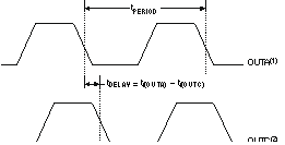
1. Also applies to OUTB.
2. Also applies to OUTD.
Figure 1. OUTA/OUTC Output Delay
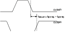
1. Also applies to OUTC.
2. Also applies to OUTD.
Figure 2. OUTA/OUTB Output Delay
5.6 Typical Characteristics
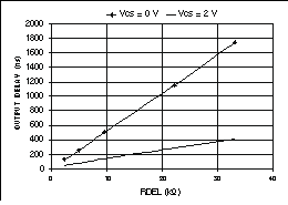
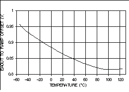
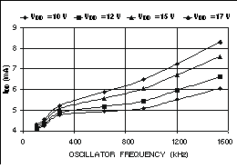
(No Output Loading)
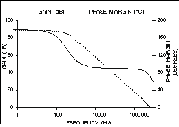
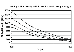
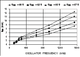
(With 0.1-Nf Output Loads)