ZHCSIU2K June 2001 – November 2023 UCC27323 , UCC27324 , UCC27325 , UCC37323 , UCC37324 , UCC37325
PRODUCTION DATA
- 1
- 1 特性
- 2 应用
- 3 说明
- 4 Device Comparison Table
- 5 Pin Configuration and Functions
- 6 Specifications
- 7 Detailed Description
- 8 Application and Implementation
- 9 Power Supply Recommendations
- 10Layout
- 11Device and Documentation Support
- 12Revision History
- 13Mechanical, Packaging, and Orderable Information
封装选项
机械数据 (封装 | 引脚)
散热焊盘机械数据 (封装 | 引脚)
- DGN|8
订购信息
8.2.2.2 Parallel Outputs
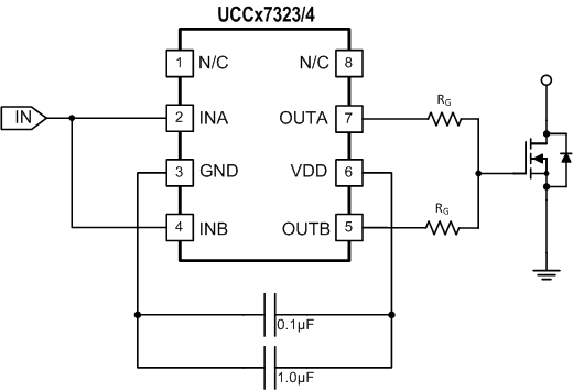
The A and B drivers may be combined into a single driver by connecting the INA/INB inputs together as close to the IC as possible, and the OUTA/OUTB outputs ties together if the external gate drive resistor is not used. In some cases where the external gate drive resistor is used, Ti recommends that the resistor can be equally split in OUTA and OUTB respectively to reduce the parasitic inductance induce unbalance between two channels, as show in Figure 8-4.
 Figure 8-4 Parallel Operation of UCCx7323 and UCCx7324
Important consideration about paralleling two channels for UCCx7323/4 include: 1) INA and INB should be shorted in PCB layout as close to the device as possible, as well as for OUTA and OUTB, in which condition PCB layout parasitic mismatching between two channels could be minimized. 2) INA/B input slope signal should be fast enough to avoid mismatched VIN_H/VIN_L, td1/td2 between channel-A and channel-B. TI recommends having input signal slope faster than 20 V/us.