ZHCSDP7 May 2015 UCC27201A-Q1
PRODUCTION DATA.
10 Layout
10.1 Layout Guidelines
To improve the switching characteristics and efficiency of a design, the following layout rules should be followed.
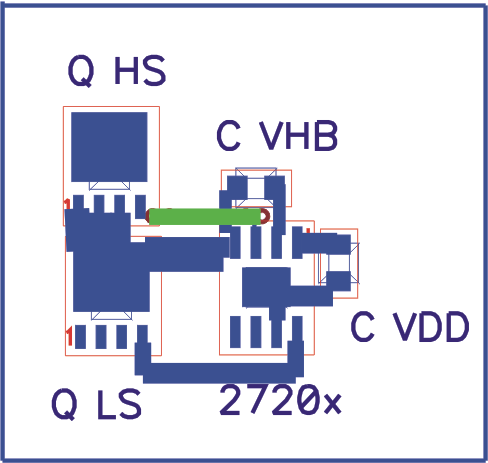
- Locate the driver as close as possible to the MOSFETs.
- Locate the VDD and VHB (bootstrap) capacitors as close as possible to the driver.
- Pay close attention to the GND trace. Use the thermal pad of the DDA package as GND by connecting it to the VSS pin (GND). Note: The GND trace from the driver goes directly to the source of the MOSFET but should not be in the high current path of the MOSFET(S) drain or source current.
- Use similar rules for the HS node as for GND for the high side driver.
- Use wide traces for LO and HO closely following the associated GND or HS traces. 60 mil to 100 mil width is preferable where possible.
- Use as least two or more vias if the driver outputs or SW node needs to be routed from one layer to another. For GND the number of vias needs to be a consideration of the thermal pad requirements as well as parasitic inductance.
- Avoid LI and HI (driver input) going close to the HS node or any other high dV/dT traces that can induce significant noise into the relatively high impedance leads.
- Keep in mind that a poor layout can cause a significant drop in efficiency versus a good PCB layout and can even lead to decreased reliability of the whole system.
10.2 Layout Example
 Figure 31. Example Component Placement