ZHCSQX4F August 1995 – August 2022 UC1823A , UC1825A , UC2823A , UC2823B , UC2825A , UC2825B , UC3823A , UC3823B , UC3825A , UC3825B
PRODUCTION DATA
- 1特性
- 2说明
- 3Revision History
- 4Ordering Information
- 5Pin Configuration and Functions
- 6Specifications
- 7Application and Implementation
- 8Device and Documentation Support
- 9Mechanical, Packaging, and Orderable Information
封装选项
请参考 PDF 数据表获取器件具体的封装图。
机械数据 (封装 | 引脚)
- DW|16
- N|16
散热焊盘机械数据 (封装 | 引脚)
订购信息
7.3 ACTIVE LOW OUTPUTS DURING UVLO
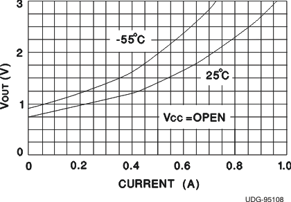
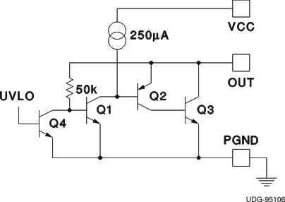
The UVLO function forces the outputs to be low and considers both VCC and VREF before allowing the chip to operate.
 Figure 7-3 Output Voltage vs Output Current
 Figure 7-4 Output V and I During UVLO