SLUS352C January 1997 – December 2015 UC1846 , UC2846 , UC3846 , UC3847
PRODUCTION DATA.
- 1 Features
- 2 Applications
- 3 Description
- 4 Revision History
- 5 Pin Configuration and Functions
- 6 Specifications
- 7 Detailed Description
- 8 Application and Implementation
- 9 Power Supply Recommendations
- 10Layout
- 11Device and Documentation Support
- 12Mechanical, Packaging, and Orderable Information
封装选项
请参考 PDF 数据表获取器件具体的封装图。
机械数据 (封装 | 引脚)
- J|16
- FK|20
散热焊盘机械数据 (封装 | 引脚)
订购信息
5 Pin Configuration and Functions
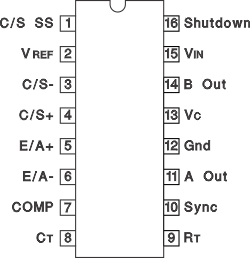
J or N, DW Packages
16-Pin CDIP or PDIP, SOIC
Top View

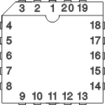
FN or FK Packages
20-Pin PLCC or LCCC
Top View

Pin Functions
| PIN | I/O | DESCRIPTION | ||
|---|---|---|---|---|
| DIL, SOIC NO. | PLCC, LCC NO. | NAME | ||
| 1 | 2 | C/S SS | I | Current limit/soft-start programming |
| 2 | 3 | VREF | O | 5.1-V reference voltage output |
| 3 | 4 | C/S – | I | Current sense comparator inverting input |
| 4 | 5 | C/S + | I | Current sense comparator non-inverting input |
| 5 | 7 | E/A + | I | Error amplifier inverting input |
| 6 | 8 | E/A – | I | Error amplifier inverting input |
| 7 | 9 | COMP | I/O | Error amplifier output and input to the PWM comparator |
| 8 | 10 | CT | I | Oscillator frequency programming capacitor pin |
| 9 | 12 | CR | I | Oscillator frequency programming resistor pin |
| 10 | 13 | Sync | I/O | Synchronization out from master controller or input of slave controller |
| 11 | 14 | A Out | O | PWM drive signal output A, Pin11 and P14 are complementary |
| 12 | 15 | GND | G | All signals are referenced to this node |
| 13 | 17 | VC | I | Bias supply input for output stage |
| 14 | 18 | B Out | O | PWM drive signal output B, Pin11 and P14 are complementary |
| 15 | 19 | VIN | I | Bias supply input |
| 16 | 20 | Shutdown | I | External shutdown signal input |
| — | 1, 6, 11, 16 | N/C | ||