ZHCSI11A August 2009 – April 2018 TXB0106-Q1
PRODUCTION DATA.
- 1 特性
- 2 应用
- 3 说明
- 4 修订历史记录
- 5 Pin Configuration and Functions
-
6 Specifications
- 6.1 Absolute Maximum Ratings
- 6.2 ESD Ratings
- 6.3 Recommended Operating Conditions
- 6.4 Thermal Information
- 6.5 Electrical Characteristics
- 6.6 Timing Requirements – VCCA = 1.2 V, TA = 25°C
- 6.7 Timing Requirements – VCCA = 1.5 V ± 0.1 V
- 6.8 Timing Requirements – VCCA = 1.8 V ± 0.15 V
- 6.9 Timing Requirements – VCCA = 2.5 V ± 0.2 V
- 6.10 Timing Requirements – VCCA = 3.3 V ± 0.3 V
- 6.11 Switching Characteristics –VCCA = 1.2 V, TA = 25°C
- 6.12 Switching Characteristics – VCCA = 1.5 V ± 0.1 V
- 6.13 Switching Characteristics – VCCA = 1.8 V ± 0.15 V
- 6.14 Switching Characteristics – VCCA = 2.5 V ± 0.2 V
- 6.15 Switching Characteristics – VCCA = 3.3 V ± 0.3 V
- 6.16 Operating Characteristics
- 6.17 Typical Characteristics
- 7 Parameter Measurement Information
- 8 Detailed Description
- 9 Application and Implementation
- 10Power Supply Recommendations
- 11Layout
- 12器件和文档支持
- 13机械、封装和可订购信息
8.3.2 Input Driver Requirements
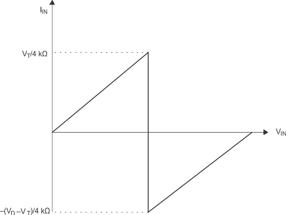
Typical IIN vs VIN characteristics of the TXB0106-Q1 device are shown in Figure 6. For proper operation, the device driving the data I/Os of the TXB0106-Q1 device must have drive strength of at least ±2 mA.

A. VT is the input threshold voltage of the TXB0106-Q1 device (typically VCCI / 2).
B. VD is the supply voltage of the external driver.
Figure 6. Typical IIN vs VIN Curve