ZHCSEG8F December 2015 – December 2023 TUSB542
PRODUCTION DATA
- 1
- 1 特性
- 2 应用
- 3 说明
- 4 Pin Configuration and Functions
-
5 Specifications
- 5.1 Absolute Maximum Ratings
- 5.2 ESD Ratings
- 5.3 Recommended Operating Conditions
- 5.4 Thermal Information
- 5.5 Electrical Characteristics, Power Supply Currents
- 5.6 Electrical Characteristics, DC
- 5.7 Electrical Characteristics, Dynamic
- 5.8 Electrical Characteristics, AC
- 5.9 Timing Requirements
- 5.10 Switching Characteristics
- 5.11 Typical Characteristics
- 6 Detailed Description
- 7 Application and Implementation
- 8 Device and Documentation Support
- 9 Revision History
- 10Mechanical, Packaging, and Orderable Information
4 Pin Configuration and Functions
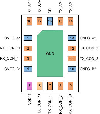
 Figure 4-1 RWQ Package,18-Pin X2QFN(Top View)
Table 4-1 Pin Functions
| PIN | TYPE | DESCRIPTION | |
|---|---|---|---|
| NAME | NO. | ||
| VDD18 | 5 | P | 1.8V Power Supply |
| GND | PAD | G | Reference Ground Thermal Pad. Must connect to GND on the board. |
| SEL | 16 | Input | 2:1 SS MUX control. See Table 1 for signal path
settings.210kΩ internal pullup resistor. H: AP SS signals are connected to Type-C position 1 signals. L: AP SS signals are connected to Type-C position 2 signals |
| CNFG_A1 | 1 | Tri-level Input | Tri-level configuration input pin A1 (for Ch 1): sets channel 1 (AP to redriver) EQ, DE and OS configurations. Pin has integrated pull-up and pull-down resistors of 105kΩ. Refer to Table 6-2 for configuration settings. |
| CNFG_B1 | 4 | Tri-level Input | Tri-level configuration input pin B1 (for Ch 1): sets channel 1 (AP to redriver) EQ, DE and OS configurations. Pin has integrated pull-up and pull-down resistors of 105kΩ. Refer to Table 6-2 for configuration settings. |
| CNFG_A2 | 13 | Tri-level Input | Tri-level configuration input pin A2 (for Ch 2): sets channel 2 (redriver to device) EQ, DE and OS configurations. Pin has integrated pull-up and pull-down resistors of 10 5kΩ. Refer to Table 6-2 for configuration settings. |
| CNFG_B2 | 10 | Tri-level Input | Tri-level configuration input pin B2 (for Ch 2): sets channel 2 (redriver to device) EQ, DE and OS configurations. Pin has integrated pull-up and pull-down resistors of 105kΩ. Refer to Table 6-2 for configuration settings. |
| RX_AP+ | 18 | Diff output | Differential output to Application Processor (AP), 5 Gbps SS positive signal |
| RX_AP- | 17 | Diff output | Differential output to AP, 5Gbps SS negative signal |
| TX_AP+ | 15 | Diff input | Differential input from AP, 5Gbps SS positive signal |
| TX_AP- | 14 | Diff input | Differential input from AP, 5Gbps SS negative signal |
| Rx_Con_1+ | 2 | Diff input | Differential input from Type-C Connector, Position 1, SS positive signal |
| Rx_Con_1- | 3 | Diff input | Differential input from Type-C Connector, Position 1, SS negative signal |
| Tx_Con_1+ | 6 | Diff output | Differential output to Type-C Connector, Position 1, SS positive signal |
| Tx_Con_1- | 7 | Diff output | Differential output to Type-C Connector, Position 1, SS negative signal |
| Rx_Con_2- | 8 | Diff input | Differential input from Type-C Connector, Position 2, SS negative signal |
| Rx_Con_2+ | 9 | Diff input | Differential input from Type-C Connector, Position 2, SS positive signal |
| Tx_Con_2+ | 12 | Diff output | Differential output to Type-C Connector, Position 2, SS positive signal |
| Tx_Con_2- | 11 | Diff output | Differential output to Type-C Connector, Position 2, SS negative signal |