ZHCSDU0F May   2015  – March 2022 TUSB320

PRODUCTION DATA  

  1. 特性
  2. 应用
  3. 说明
  4. Revision History
  5. Pin Configuration and Functions
  6. Specifications
    1. 6.1 Absolute Maximum Ratings
    2. 6.2 ESD Ratings
    3. 6.3 Recommended Operating Conditions
    4. 6.4 Thermal Information
    5. 6.5 Electrical Characteristics
    6. 6.6 Timing Requirements
    7. 6.7 Switching Characteristics
  7. Detailed Description
    1. 7.1 Overview
    2. 7.2 Functional Block Diagram
      1. 7.2.1 Cables, Adapters, and Direct Connect Devices
        1. 7.2.1.1 USB Type-C Receptacles and Plugs
        2. 7.2.1.2 USB Type-C Cables
        3. 7.2.1.3 Legacy Cables and Adapters
        4. 7.2.1.4 Direct Connect Devices
        5. 7.2.1.5 Audio Adapters
    3. 7.3 Feature Description
      1. 7.3.1 Port Role Configuration
        1. 7.3.1.1 Downstream Facing Port (DFP) – Source
        2. 7.3.1.2 Upstream Facing Port (UFP) – Sink
        3. 7.3.1.3 Dual Role Port (DRP)
      2. 7.3.2 Type-C Current Mode
      3. 7.3.3 Accessory Support
        1. 7.3.3.1 Audio Accessory
        2. 7.3.3.2 Debug Accessory
      4. 7.3.4 I2C and GPIO Control
      5. 7.3.5 VBUS Detection
    4. 7.4 Device Functional Modes
      1. 7.4.1 Unattached Mode
      2. 7.4.2 Active Mode
      3. 7.4.3 Dead Battery Mode
      4. 7.4.4 Shutdown Mode
    5. 7.5 Programming
    6. 7.6 Register Maps
  8. Application and Implementation
    1. 8.1 Application Information
    2. 8.2 Typical Application
      1. 8.2.1 DRP in I2C Mode
        1. 8.2.1.1 Design Requirements
        2. 8.2.1.2 Detailed Design Procedure
        3. 8.2.1.3 Application Curves
      2. 8.2.2 DFP in I2C Mode
        1. 8.2.2.1 Design Requirements
        2. 8.2.2.2 Detailed Design Procedure
        3. 8.2.2.3 Application Curves
      3. 8.2.3 UFP in I2C Mode
        1. 8.2.3.1 Design Requirements
        2. 8.2.3.2 Detailed Design Procedure
        3. 8.2.3.3 Application Curves
    3. 8.3 Initialization Set Up
  9. Power Supply Recommendations
  10. 10Layout
    1. 10.1 Layout Guidelines
    2. 10.2 Layout Example
  11. 11Device and Documentation Support
    1. 11.1 接收文档更新通知
    2. 11.2 支持资源
    3. 11.3 Trademarks
    4. 11.4 Electrostatic Discharge Caution
    5. 11.5 术语表
  12. 12Mechanical, Packaging, and Orderable Information

封装选项

机械数据 (封装 | 引脚)
散热焊盘机械数据 (封装 | 引脚)
订购信息

Switching Characteristics

over operating free-air temperature range (unless otherwise noted)
PARAMETERTEST CONDITIONSMINTYPMAXUNIT
tCCCB_DEFAULTPower on default of CC1 and CC2 voltage debounce timeDEBOUCE
register = 2'b00
133ms
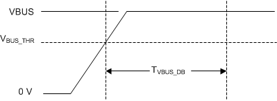
tVBUS_DBDebounce of VBUS_DET pin after valid VBUS_THR2ms
tDRP_DUTY_CYCLEPower-on default of percentage of time DRP advertises DFP during a tDRPDRP_DUTY_CYCLE register = 2'b0030%
tDRPThe period during which the TUSB320 or the TUSB320I in DFP mode completes a DFP to UFP and back advertisement.5075100ms
tI2C_ENTime from TUSB320 EN_N low or TUSB320I EN high and VDD active to I2C access available100ms
tSOFT_RESETSoft reset duration264995ms
GUID-4168D514-DAE7-4458-A504-7E60C8A72485-low.gif Figure 6-1 VBUS Detect and Debounce