ZHCS460C October 2011 – August 2015 TS3USBA225
PRODUCTION DATA.
7 Detailed Description
7.1 Overview
The TS3USBA225 is a 2-channel single-pole triple-throw (SP3T) multiplexer that supports USB 2.0 High-Speed (480 Mbps) signals in all 3 differential channels. The first two high-speed differential channels also support Mobile High Definition Link (MHL) signaling with video resolution and frame rates up to 720p, 60 fps and 1080i, 30 fps. The remaining differential channel can also be used as an audio switch that is designed to allow analog audio signals to swing negatively. This configuration allows the system designer to use a common connector for audio and USB 2.0 or MHL data.
The TS3USBA225 has a VCC range of 2.7 V to 5.0 V with the capability to pass true-ground audio signals down to –1.8 V. The device also supports a power-down mode that can be enabled when both SEL controls are low to minimize current consumption when no signal is transmitting. The TS3USBA225 also features internal shunt resistors on the audio path to reduce clicks and pops that may be heard when the audio switches are selected.
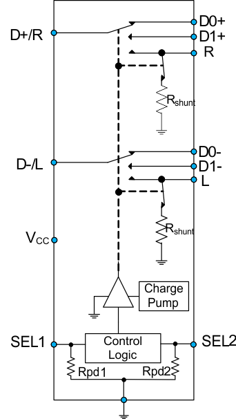
7.2 Functional Block Diagram

7.3 Feature Description
7.3.1 Click and Pop Reduction
The shunt resistors in the TS3USBA225 automatically discharge any capacitance at the L and R terminals when they are not connected to the common D-/L and D+/R paths. This reduces the audible click-and-pop sounds that occur when switching between audio sources. Audible clicks and pops are caused when a step DC voltage is switched into the speaker. By automatically discharging the side that is not connected, any residual DC voltage is removed, thereby reducing the clicks and pops.
7.3.2 Negative Signal Swing Capability
The TS3USBA225 has an analog audio path L and R that can support negative signals that pass below ground without distortion. These analog switches operate from –1.8 V to 4.3 V.
7.4 Device Functional Modes
7.4.1 High Impedance (Hi-Z) Mode
The TS3USBA225 has a Hi-Z mode that places the device's signal paths in a high impedance state when there is no power supplied to the TS3USBA225 VCC pin. This mode will isolate the signal bus in a powered off situation so that it may not interfere with other devices that maybe sharing the bus.
7.4.1.1 Power-Down Mode
The TS3USBA225 has a power-down mode that reduces the power consumption to 3 μA when the device is not in use. To put the device in power-down mode and disable the switch, the SEL1 and SEL2 pins must be supplied with a logic low signal.
7.4.2 Device Functional Modes
Table 1 is the function table for the TS3USBA225.