ZHCSBM1C September 2013 – March 2017 TS3USB3031
PRODUCTION DATA.
9 Application and Implementation
NOTE
Information in the following applications sections is not part of the TI component specification, and TI does not warrant its accuracy or completeness. TI’s customers are responsible for determining suitability of components for their purposes. Customers should validate and test their design implementation to confirm system functionality.
9.1 Application Information
The TS3USB3031 is a passive, bidirectional, 2-channel 1:3 switch which makes it versatile to be used in many high speed 1:3 switching applications. This device was designed originally for USB 2.0 and Mobile High-Definition Link applications but can be used for general signal switching applications such as I2C, UART, LVDS, and so forth.
9.2 Typical Application
Figure 14 represents a typical application of the TS3USB3031 MHL switch. The TS3USB3031 is used to switch signals between the 2 sets of USB paths, which go to either the baseband or application processor, and the MHL path, which goes to the HDMI to MHL bridge. The TS3USB3031 has internal 6-MΩ pulldown resistors on SEL0 and SEL1. The pulldown on SEL0 and SEL1 ensure the USB1 channel is selected by default. The TS5A3157 is a separate SPDT switch that is used to switch between MHL’s CBUS and the USB ID line that is required for USB OTG (USB On-The-Go) application.
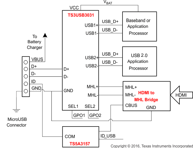 Figure 14. Typical TS3USB3031 Application
9.2.1 Design Requirements
Design requirements of the MHL and USB 1.0,1.1, and 2.0 standards must be followed.
The TS3USB3031 has internal 6-MΩ pulldown resistors on SEL0 and SEL1 so no external resistors are required on the logic pins. The pulldown on SEL0 and SEL1 ensure the USB1 channel is selected by default.
The TS5A3157 is a separate SPDT switch that is used to switch between the CBUS of the MHL and the USB ID line that is required for USB OTG (USB On-The-Go) application.
9.2.2 Detailed Design Procedure
The TS3USB3031 can be properly operated without any external components. However, TI recommends that unused signal I/O pins must be connected to ground through a 50-Ω resistor to prevent signal reflections back into the device.
9.2.3 Application Curves
9.2.3.1 MHL Eye Pattern
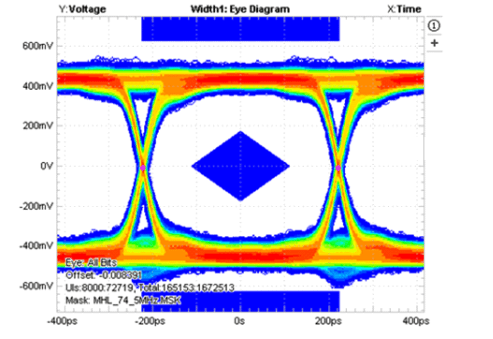 Figure 15. Eye Pattern Error Histogram: 2.25 Gbps
With No Device
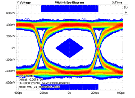 Figure 17. Eye Pattern Error Histogram: 2.25 Gbps
With TS3USB3031 (Added Jitter = 5.04 ps)
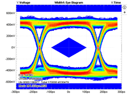 Figure 19. Eye Pattern Error Histogram: 3.0 Gbps
With No Device
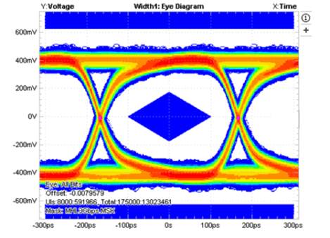 Figure 21. Eye Pattern Error Histogram: 3.0 Gbps
With TS3USB3031 (Added Jitter = 2.57 ps)
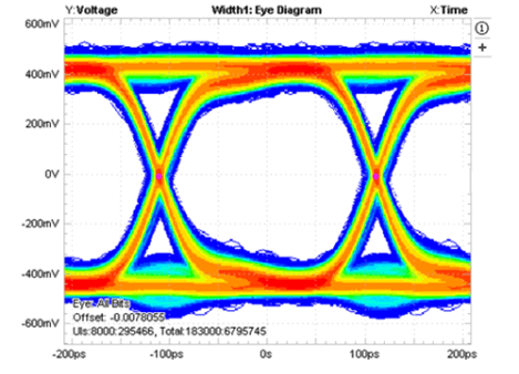 Figure 23. Eye Pattern Error Histogram: 4.5 Gbps
With No Device
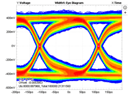 Figure 25. Eye Pattern Error Histogram: 4.5 Gbps
With TS3USB3031 (Added Jitter = 1.13 ps)
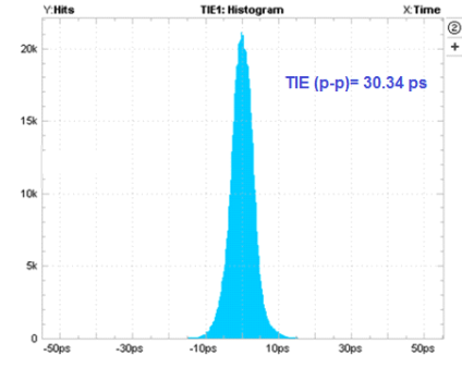 Figure 16. Time Interval Error Histogram: 2.25 Gbps
With No Device
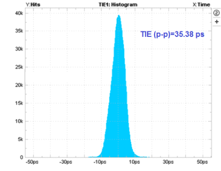 Figure 18. Time Interval Error Histogram: 2.25 Gbps
 With TS3USB3031 (Added Jitter = 5.04 ps)
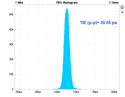 Figure 20. Time Interval Error Histogram: 3.0 Gbps
With No Device
 Figure 22. Time Interval Error Histogram: 3.0 Gbps
With TS3USB3031 (Added Jitter = 2.57 ps)
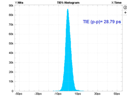 Figure 24. Time Interval Error Histogram: 4.5 Gbps
With No Device
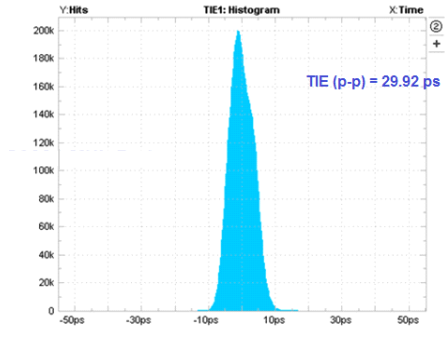 Figure 26. Time Interval Error Histogram: 4.5 Gbps
With TS3USB3031 (Added Jitter = 1.13 ps)
9.2.3.2 USB EYE Pattern
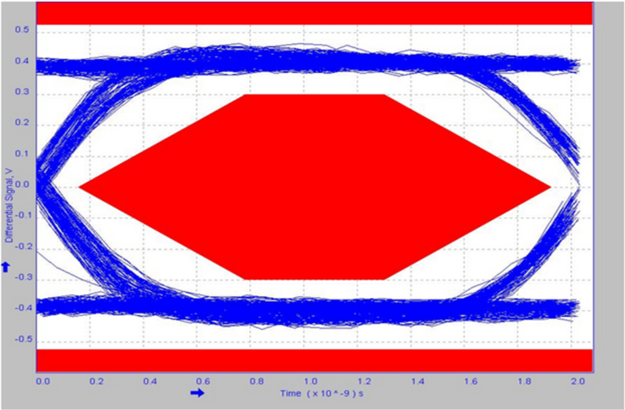 Figure 27. 480-Mbps USB 2.0 Eye Pattern With No Device
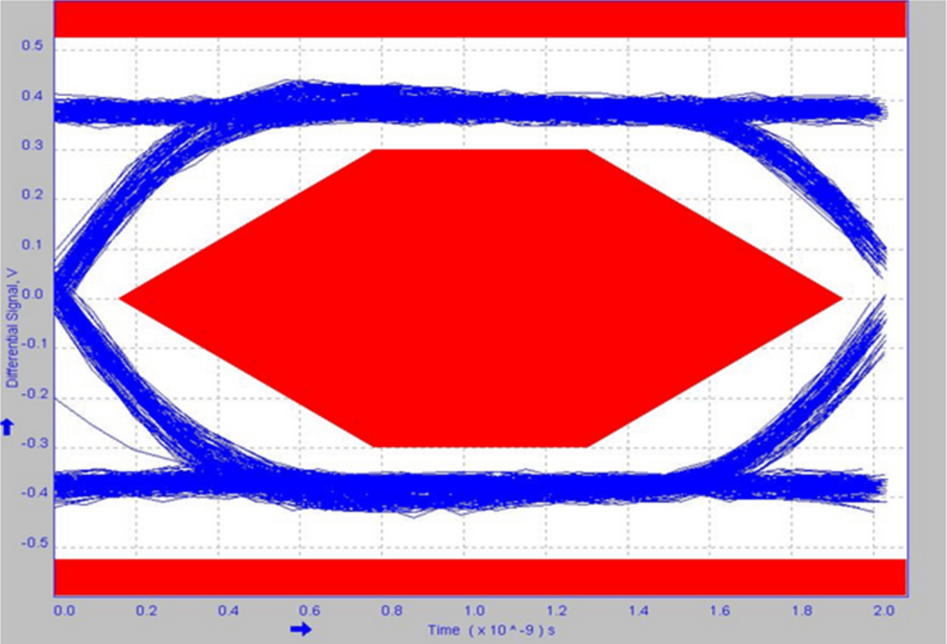 Figure 28. 480-Mbps USB 2.0 Eye Pattern for USB Switch