ZHCSEZ3C May   2016  – May 2016 TRS3122E

PRODUCTION DATA.  

  1. 特性
  2. 应用
  3. 说明
  4. 修订历史记录
  5. Pin Configuration and Functions
  6. Specifications
    1. 6.1  Absolute Maximum Ratings
    2. 6.2  ESD Ratings
    3. 6.3  Recommended Operating Conditions
    4. 6.4  Thermal Characteristics
    5. 6.5  Power and Status Electrical Characteristics
    6. 6.6  Driver Electrical Characteristics
    7. 6.7  Receiver Electrical Characteristics
    8. 6.8  Driver Switching Characteristics
    9. 6.9  Receiver Switching Characteristics
    10. 6.10 Power and Status Switching Characteristics
    11. 6.11 Typical Characteristics
  7. Parameter Measurement Information
  8. Detailed Description
    1. 8.1 Overview
    2. 8.2 Functional Block Diagram
    3. 8.3 Feature Description
      1. 8.3.1 Charge Pump
        1. 8.3.1.1 Doubler Mode
        2. 8.3.1.2 Tripler Mode
      2. 8.3.2 Drivers
      3. 8.3.3 Receivers
      4. 8.3.4 ESD Protection
      5. 8.3.5 Auto Powerdown Plus
        1. 8.3.5.1 Automatic Powerdown
        2. 8.3.5.2 Manual Powerdown
        3. 8.3.5.3 Forced On
    4. 8.4 Device Functional Modes
      1. 8.4.1 Each Driver
      2. 8.4.2 Each Receiver
      3. 8.4.3 INVALID Status Truth Table
      4. 8.4.4 Capacitor Selection Table
  9. Application and Implementation
    1. 9.1 Application Information
    2. 9.2 Typical 1.8-V Application
      1. 9.2.1 Design Requirements
      2. 9.2.2 Detailed Design Procedure
        1. 9.2.2.1 Data-Rate and Cable Length
        2. 9.2.2.2 Capacitor Selection
      3. 9.2.3 Application Curves
  10. 10Power Supply Recommendations
  11. 11Layout
    1. 11.1 Layout Guidelines
    2. 11.2 Layout Example
  12. 12器件和文档支持
    1. 12.1 器件支持
      1. 12.1.1 Third-Party Products Disclaimer
    2. 12.2 社区资源
    3. 12.3 商标
    4. 12.4 静电放电警告
    5. 12.5 Glossary
  13. 13机械、封装和可订购信息

封装选项

机械数据 (封装 | 引脚)
散热焊盘机械数据 (封装 | 引脚)
订购信息

5 Pin Configuration and Functions

VQFN P Package
24-Pin RGE
Top View
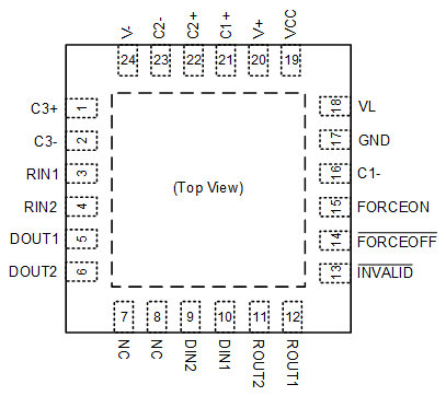
TRS3122E RGE_po.gif

Pin Functions

Pin I/O DESCRIPTION
NAME NO.
C1+, C2+ 21, 22 - Positive terminals of voltage-doubler charge-pump capacitors (required)
C3+ 1 - Positive terminal of voltage-tripler charge-pump capacitor (Not needed for VCC 3V to 5.5V)
C1–, C2- 16, 23 - Negative terminals of voltage-doubler charge-pump capacitors (required)
C3- 2 - Negative terminal of voltage-tripler charge-pump capacitor (Not needed for VCC 3V to 5.5V)
V+ 20 - Positive charge pump storage capacitor (required)
V– 24 - Negative charge pump storage capacitor (required)
GND 17 - Ground
VCC 19 - 1.8-V or 3-V to 5-V supply voltage
VL 18 - Logic-level supply. All CMOS inputs (DIN) and outputs (ROUT) are referenced to this supply.
FORCEOFF 14 I Auto Powerdown Control input (Refer to Truth Table)
FORCEON 15 I Auto Powerdown Control input (Refer to Truth Table)
INVALID 13 O Invalid Output Pin
DIN1, DIN2 10,9 I Driver inputs
DOUT1, DOUT2 5, 6 O RS-232 driver outputs
RIN1, RIN2 3, 4 I RS-232 receiver inputs
ROUT1, ROUT2 12, 11 O Receiver outputs; swing between 0 and VL
NC 7, 8 I Factory pins, can be unconnected or connected to GND