ZHCSEC7A October 2012 – October 2015 TPS92640 , TPS92641
PRODUCTION DATA.
- 1 特性
- 2 应用
- 3 说明
- 4 修订历史记录
- 5 Pin Configuration and Functions
- 6 Specifications
-
7 Detailed Description
- 7.1 Overview
- 7.2 Functional Block Diagram
- 7.3
Feature Description
- 7.3.1 Controlled On-Time Architecture
- 7.3.2 Switching Frequency
- 7.3.3 Average LED Current
- 7.3.4 Analog Dimming and True-Zero Operation
- 7.3.5 Undervoltage Lockout (UVLO)
- 7.3.6 PWM Dimming Using the UDIM Pin
- 7.3.7 External Shunt FET PWM Dimming
- 7.3.8 VCC Regulation and Start-up
- 7.3.9 Precision Reference
- 7.3.10 Control Loop Compensation
- 7.3.11 Overcurrent Protection
- 7.3.12 Overvoltage Protection (OVP)
- 7.3.13 Boot Undervoltage Lockout (UVLO)
- 7.4 Device Functional Modes
-
8 Application and Implementation
- 8.1 Application Information
- 8.2
Typical Applications
- 8.2.1
TPS92640: Design Procedure
- 8.2.1.1 Design Requirements
- 8.2.1.2
Detailed Design Procedure
- 8.2.1.2.1 Set Output Voltage Feedback Ratio
- 8.2.1.2.2 Set Switching Frequency
- 8.2.1.2.3 Set Average LED Current
- 8.2.1.2.4 Set Inductor Ripple Current
- 8.2.1.2.5 Set LED Ripple Current and Determine Output Capacitance, COUT
- 8.2.1.2.6 Choose N-Channel MOSFETs
- 8.2.1.2.7 Choose Input Capacitance
- 8.2.1.2.8 Set the Turnon Voltage and Undervoltage Lockout Hysteresis
- 8.2.2
TPS92640 - PWM Dimming Application
- 8.2.2.1 Design Requirements
- 8.2.2.2
Detailed Design Procedure
- 8.2.2.2.1 Calculate Operating Points
- 8.2.2.2.2 Output Voltage Feedback
- 8.2.2.2.3 Switching Frequency
- 8.2.2.2.4 Set the Feedback Reference and LED Current
- 8.2.2.2.5 Calculate the Inductor Value
- 8.2.2.2.6 Calculate the Output Capacitor Value
- 8.2.2.2.7 Calculate the MOSFET Parameters
- 8.2.2.2.8 Calculate the Minimum Input Capacitance
- 8.2.2.2.9 Undervoltage Lockout and Hysteresis
- 8.2.2.3 Application Curve
- 8.2.1
TPS92640: Design Procedure
- 9 Power Supply Recommendations
- 10Layout
- 11器件和文档支持
- 12机械、封装和可订购信息
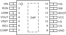
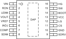
5 Pin Configuration and Functions
TPS92640 PWP Package
14-Pin HTSSOP
Top View

TPS92641 PWP Package
16-Pin HTSSOP
Top View

Pin Functions
| PIN | I/O | DESCRIPTION | ||
|---|---|---|---|---|
| NAME | NO. (TPS92640) | NO. (TPS92641) | ||
| BOOT | 12 | 14 | O | Connect 100-nF ceramic capacitor to switch node and diode to VCC to provide boosted voltage for high-side gate drive. |
| COMP | 7 | 7 | O | Connect ceramic capacitor to GND to set loop compensation. |
| CS | 9 | 11 | I | Connect to positive terminal of sense resistor at the bottom of the LED stack. |
| GND | 8 | 10 | — | System GND. Connect to DAP. |
| HG | 14 | 16 | O | Connect to gate of high-side NFET of buck regulator. Use series resistor to limit current slew-rate and mitigate EMI noise. |
| IADJ | 6 | 6 | I | Connect resistor divider from VREF to set analog dimming level. Use NTC resistor from pin to GND as resistor divider to implement thermal foldback operation. |
| LG | 10 | 12 | O | Connect to gate of low-side NFET of buck regulator. Use series resistor to limit current slew-rate and mitigate EMI noise. |
| RON | 2 | 2 | I | Connect a resistor to VIN and capacitor to GND to set switching frequency. |
| SDIM | — | 8 | I | PWM dimming input for shunt FET dimming. |
| SDRV | — | 9 | O | Connect to gate of external parallel NFET across LED load used for shunt dimming if desired. |
| SW | 13 | 15 | O | Connect to switch node of buck regulator. |
| UDIM | 3 | 3 | I | Connect resistor divider from VIN to set undervoltage lockout threshold. |
| VCC | 11 | 13 | O | Bypass with 2.2-µF ceramic capacitor to provide bias supply for controller. |
| VIN | 1 | 1 | I | Connect to input voltage. Connect 1-µF bypass capacitor |
| VOUT | 4 | 4 | I | Connect resistor divider from VOUT, scaled down feedback of VOUT. |
| VREF | 5 | 5 | O | System reference voltage. Bypass with 100-nF ceramic capacitor. |
| DAP | — | — | — | Place 6-9 vias from pad to GND plane for thermal relief. |