ZHCSEI3A January 2016 – February 2017 TPS7H1101-SP
PRODUCTION DATA.
- 1 特性
- 2 应用
- 3 说明
- 4 修订历史记录
- 5 说明 (续)
- 6 Pin Configuration and Functions
- 7 Specifications
- 8 Detailed Description
- 9 Application and Implementation
- 10Power Supply Recommendations
- 11Layout
- 12器件和文档支持
- 13机械、封装和可订购信息
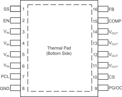
6 Pin Configuration and Functions
HKR Package
16-Pin CFP
Bottom View

Pin Functions
| PIN | I/O | DESCRIPTION | |
|---|---|---|---|
| NAME | NO. | ||
| SS | 1 | O | Soft-start terminal. Connecting an external capacitor slows down the output voltage ramp rate after enable event. The soft-start terminal can be used to disable the device as described in theSoft Start section. |
| EN | 2 | I | Enable terminal. Driving this terminal to logic high enables the device; driving the terminal to logic low disables the device. VIN voltage must be greater than 3.5 V when using the EN pin. For VIN < 3.5 V, enable terminal cannot be used to disable the device. TI recommends to connect the enable terminal to VIN. |
| VIN | 3 | I | Unregulated supply voltage. TI recommends to connect an input capacitor as a good analog circuit practice. |
| 4 | |||
| 5 | |||
| 6 | |||
| PCL | 7 | O | Programmable current limit. A resistor to GND sets the overcurrent limit activation point. The range of resistor that can be used on the PCL terminal to GND is 8.2 kΩ to 160 kΩ. |
| GND | 8 | — | Ground/thermal pad.(1) |
| PG/OC | 9 | O | Power Good terminal. PG is an open-drain output to indicate the output voltage reaches 90% of target. PG terminal is also used as indicator when an overcurrent condition is activated. PG pin should have a pull-up resistor to the VOUT pin. |
| CS | 10 | O | Current sense terminal. Resistor connected from CS to VIN. CS terminal indicates voltage proportional to output current.
CS terminal low: Foldback current limit disabled CS terminal high: Foldback current limit enabled |
| VOUT | 11 | O | Regulated output. |
| 12 | |||
| 13 | |||
| 14 | |||
| COMP | 15 | I | Internal compensation point for error amplifier. |
| FB | 16 | I | The output voltage feedback input through voltage dividers. See Adjustable Output Voltage (Feedback Circuit) section. |
(1) Thermal pad must be connected to GND.