ZHCSE23A January 2015 – August 2015 TPS7B4253-Q1
PRODUCTION DATA.
- 1 特性
- 2 应用
- 3 说明
- 4 修订历史记录
- 5 Pin Configuration and Functions
- 6 Specifications
-
7 Detailed Description
- 7.1 Overview
- 7.2 Functional Block Diagram
- 7.3 Feature Description
- 7.4 Device Functional Modes
- 8 Application and Implementation
- 9 Power Supply Recommendations
- 10Layout
- 11器件和文档支持
- 12机械、封装和可订购信息
封装选项
机械数据 (封装 | 引脚)
散热焊盘机械数据 (封装 | 引脚)
订购信息
10 Layout
10.1 Layout Guidelines
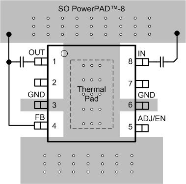
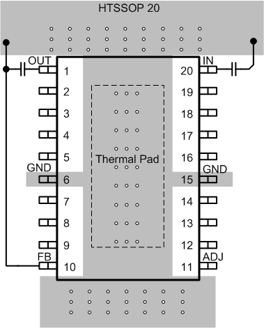
For the layout of the TPS7B4253-Q1 device, place the input and output capacitors close to the devices as shown in the Functional Block Diagram. To enhance the thermal performance, TI recommends surrounding the device with some vias.
Minimize equivalent series inductance (ESL) and ESR to maximize performance and ensure stability. Place every capacitor as close as possible to the device and on the same side of the PCB as the regulator.
Do not place any of the capacitors on the opposite side of the PCB from where the regulator is installed. TI strongly discourages the use of vias and long traces for the path between the output capacitor and the OUT pins because vias can negatively impact system performance and even cause instability.
If possible, and to ensure the maximum performance specified in this data sheet, use the same layout pattern used for the TPS7B4253-Q1 evaluation board, TPS7B4253EVM, which is available at
www.ti.com/tool/TPS7B4253EVM.
10.2 Layout Example
 Figure 31. SO PowerPAD Package TPS7B4253-Q1 Layout Example
 Figure 32. HTSSOP Package TPS7B4253-Q1 Layout Example
10.3 Power Dissipation and Thermal Considerations
Use Equation 5 to calculate the device power dissipation.

where
- PD = continuous power dissipation
- IO = output current
- VI = input voltage
- VO = output voltage
- IQ = quiescent current
As IQ « IO, the term IQ × VI in Equation 5 can be ignored.
For a device under operation at a given ambient air temperature (TA), calculate the junction temperature (TJ) with Equation 6.

where
- θJA = junction-to-junction-ambient air thermal impedance
A rise in junction temperature because of power dissipation can be calculated with Equation 7.

For a given maximum junction temperature (TJmax), the maximum ambient air temperature (TAmax) at which the device can operate can be calculated with Equation 8.
