ZHCSEI2B January 2016 – June 2021 TPS7A84
PRODUCTION DATA
- 1 特性
- 2 应用
- 3 说明
- 4 Revision History
- 5 Pin Configurations and Functions
- 6 Specifications
- 7 Detailed Description
-
8 Application and Implementation
- 8.1
Application Information
- 8.1.1 Recommended Capacitor Types
- 8.1.2 Input and Output Capacitor Requirements (CIN and COUT)
- 8.1.3 Noise-Reduction and Soft-Start Capacitor (CNR/SS)
- 8.1.4 Feed-Forward Capacitor (CFF)
- 8.1.5 Soft-Start and In-Rush Current
- 8.1.6 Optimizing Noise and PSRR
- 8.1.7 Charge Pump Noise
- 8.1.8 ANY-OUT Programmable Output Voltage
- 8.1.9 ANY-OUT Operation
- 8.1.10 Increasing ANY-OUT Resolution for LILO Conditions
- 8.1.11 Current Sharing
- 8.1.12 Adjustable Operation
- 8.1.13 Sequencing Requirements
- 8.1.14 Power-Good Operation
- 8.1.15 Undervoltage Lockout (UVLO) Operation
- 8.1.16 Dropout Voltage (VDO)
- 8.1.17 Behavior when Transitioning from Dropout into Regulation
- 8.1.18 Load Transient Response
- 8.1.19 Negatively-Biased Output
- 8.1.20 Reverse Current Protection
- 8.1.21 Power Dissipation (PD)
- 8.1.22 Estimating Junction Temperature
- 8.1.23 Recommended Area for Continuous Operation (RACO)
- 8.2 Typical Applications
- 8.1
Application Information
- 9 Power Supply Recommendations
- 10Layout
- 11Device and Documentation Support
- 12Mechanical, Packaging, and Orderable Information
8.1.22 Estimating Junction Temperature
The JEDEC standard now recommends the use of psi (Ψ) thermal metrics to estimate the junction temperatures of the LDO when in-circuit on a typical PCB board application. These metrics are not strictly speaking thermal resistances, but rather offer practical and relative means of estimating junction temperatures. These psi metrics are determined to be significantly independent of the copper-spreading area. The key thermal metrics (ΨJT and ΨJB) are given in the Section 6.5 table and are used in accordance with Equation 12.
Equation 12. 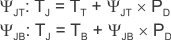
where:
- PD is the power dissipated as explained in Equation 9
- TT is the temperature at the center-top of the device package, and
- TB is the PCB surface temperature measured 1 mm from the device package and centered on the package edge