ZHCSN49M january 2007 – april 2023
PRODUCTION DATA
- 1 特性
- 2 应用
- 3 描述
- 4 Revision History
- 5 Pin Configuration and Functions
-
6 Specifications
- 6.1 Absolute Maximum Ratings
- 6.2 ESD Ratings
- 6.3 Recommended Operating Conditions
- 6.4 Thermal Information
- 6.5 Electrical Characteristics: Other Orderable Devices (non-M3 Suffix)
- 6.6 Electrical Characteristics: Orderable Device with M3 suffix
- 6.7 典型特性:IOUT = 50 mA
- 6.8 Typical Characteristics: IOUT = 1 A
- 6.9 Typical Characteristics: IOUT = 50 mA (M3 Suffix)
- 6.10 Typical Characteristics: IOUT = 1 A (M3 Suffix)
- 7 Detailed Description
- 8 Application and Implementation
- 9 Device and Documentation Support
- 10Mechanical, Packaging, and Orderable Information
封装选项
机械数据 (封装 | 引脚)
散热焊盘机械数据 (封装 | 引脚)
订购信息
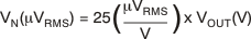
8.1.5 Output Noise
The TPS748 provides low output noise when a soft-start capacitor is used. When the device reaches the end of the soft-start cycle, the soft-start capacitor serves as a filter for the internal reference. By using a 1-nF soft-start capacitor, the output noise is reduced by half and is typically 30 μVRMS for a 1.2-V output (10 Hz to 100 kHz). Further increasing CSS has little effect on noise. Because most of the output noise is generated by the internal reference, the noise is a function of the set output voltage. The RMS noise with a 1-nF soft-start capacitor is given in Equation 5:
The low output noise of the TPS748 makes the device a good choice for powering transceivers, PLLs, or other noise-sensitive circuitry.