ZHCSDG2 March 2015 TPS65632
PRODUCTION DATA.
- 1 特性
- 2 应用范围
- 3 说明
- 4 简化电路原理图
- 5 修订历史记录
- 6 Pin Configuration and Functions
- 7 Specifications
-
8 Detailed Description
- 8.1 Overview
- 8.2 Functional Block Diagram
- 8.3 Feature Description
- 8.4 Device Functional Modes
- 9 Application and Implementation
- 10Power Supply Recommendations
- 11Layout
- 12器件和文档支持
- 13机械、封装和可订购信息
8 Detailed Description
8.1 Overview
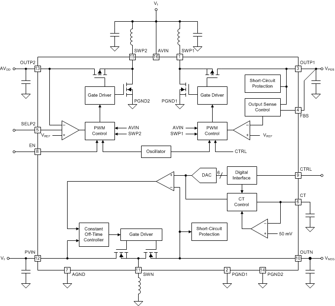
The TPS65632 consists of two boost converters and an inverting buck-boost converter. The VPOS output is fixed at 4.6 V and VNEG is programmable via a digital interface in the range of –1.4 V to –5.4 V; the default is –4 V. AVDD can be selected between 7.7 V and 5.8 V, using the SELP2 pin. The transition time of VNEG output is adjustable by the CT pin capacitor.
8.2 Functional Block Diagram

8.3 Feature Description
8.3.1 Boost Converter 1 (VPOS)
Boost converter 1 uses a fixed-frequency current-mode topology. Its output voltage (VPOS) is programmed at the factory to 4.6 V and cannot be changed by the user.
For highest output voltage accuracy, connect the output sense pin (FBS) directly to the positive terminal of the main output capacitor. If not used, the FBS pin can be left floating or connected to ground, in which case the boost converter senses the output voltage via the OUTP1 pin.
8.3.1.1 V(POS) Boost Output Sense (FBS Pin)
V(POS) boost has a dedicated output sense pin (FBS). If FBS is floating or connected to ground, V(POS) boost senses the output through OUTP1 pin.
8.3.2 Inverting Buck-Boost Converter (VNEG)
The inverting buck-boost converter uses a constant-off-time current-mode topology. The converter's default output voltage (VNEG) is –4.0 V, but it can be programmed from –1.4 V to –5.4 V (see Programming VNEG ).
8.3.2.1 Programming VNEG
The digital interface allows programming of VNEG in discrete steps. If the output voltage setting function is not required then the CTRL pin can also be used as a standard enable pin. The digital output voltage programming of VNEG is implemented using a simple digital interface with the timing shown in Figure 5.
 Figure 5. Digital Interface Using CTRL
When CTRL is pulled high the device starts up with its default voltage of –4 V. The device includes a 6-bit DAC that generates the output voltages shown in Table 1. The interface counts the rising edges applied to the CTRL pin once the device is enabled. According toTable 1, VNEG is programmed to –5.2 V since 3 rising edges are detected.
Table 1.
| Bit / Rising Edges | VNEG | DAC Value | Bit / Rising Edges | VNEG | DAC Value | |
|---|---|---|---|---|---|---|
| 0 / no pulse | –4.0 V | 000000 | 21 | –3.4 V | 010101 | |
| 1 | –5.4 V | 000001 | 22 | –3.3 V | 010110 | |
| 2 | –5.3 V | 000010 | 23 | –3.2 V | 010111 | |
| 3 | –5.2 V | 000011 | 24 | –3.1 V | 011000 | |
| 4 | –5.1 V | 000100 | 25 | –3.0 V | 011001 | |
| 5 | –5.0 V | 000101 | 26 | –2.9 V | 011010 | |
| 6 | –4.9 V | 000110 | 27 | –2.8 V | 011011 | |
| 7 | –4.8 V | 000111 | 28 | –2.7 V | 011100 | |
| 8 | –4.7 V | 001000 | 29 | –2.6 V | 011101 | |
| 9 | –4.6 V | 001001 | 30 | –2.5 V | 011110 | |
| 10 | –4.5 V | 001010 | 31 | –2.4 V | 011111 | |
| 11 | –4.4 V | 001011 | 32 | –2.3 V | 100000 | |
| 12 | –4.3 V | 001100 | 33 | –2.2 V | 100001 | |
| 13 | –4.2 V | 001101 | 34 | –2.1 V | 100010 | |
| 14 | –4.1 V | 001110 | 35 | –2.0 V | 100011 | |
| 15 | –4.0 V | 001111 | 36 | –1.9 V | 100100 | |
| 16 | –3.9 V | 010000 | 37 | –1.8 V | 100101 | |
| 17 | –3.8 V | 010001 | 38 | –1.7 V | 100110 | |
| 18 | –3.7 V | 010010 | 39 | –1.6 V | 100111 | |
| 19 | –3.6 V | 010011 | 40 | –1.5 V | 101000 | |
| 20 | –3.5 V | 010100 | 41 | –1.4 V | 101001 |
8.3.2.2 Controlling VNEG Transition Time
The transition time (tSET) is the time required to move VNEG from one voltage level to the next. Users can control the transition time with a capacitor connected between the CT pin and ground. When the CT pin is left open or connected to ground the transition time is as short as possible. When a capacitor is connected to the CT pin the transition time is determined by the time constant (τ) of the external capacitor (C(CT)) and the internal resistance of the CT pin (RCT). The output voltage reaches 70% of its programmed value after 1τ.
An example is given when using 100 nF for C(CT).
The output voltage is at 70% of its final value after 1τ (i.e. 30 ms in this case) and at its final value after approximately 3τ (90 ms in this case).
8.3.3 Boost Converter 2 (AVDD)
Boost converter 2 uses a fixed-frequency current-mode topology. The TPS65632 device supports fixed output voltages of 5.8 V and 7.7 V, selected by the SELP2 pin. AVDD = 7.7 V when SELP2 is low or left floating, and AVDD = 5.8 V when SELP2 is high.
8.3.4 Soft Start and Start-Up Sequence
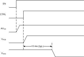
The devices feature a soft-start function to limit inrush current. Boost converter 2 (AVDD) is enabled when EN goes high. When CTRL goes high, boost converter 1 starts with a reduced switch current limit and 10 ms later the inverting buck-boost converter (VNEG) starts with its default value of –4 V. The typical start-up sequence is shown in Figure 6. The two boost converters operate independently and boost converter 1 (VPOS) does not require boost converter 2 (AVDD) to be in regulation in order for it to start..
 Figure 6. Start-Up Sequence
8.3.5 Enable (CTRL)
The CTRL pin serves two functions: one is to enable and disable the device, and the other is to program the output voltage (VNEG) of the inverting buck-boost converter (see Programming VNEG). If the VNEG programming function is not required the CTRL pin can be used as a standard enable pin for the device, which will start up with its default value of –4.0 V on VNEG. The device is enabled when CTRL is pulled high and disabled when CTRL is pulled low.
Note that to ensure proper start up CTRL must be pulled low for a minimum of 200 µs before being pulled high again.
8.3.6 Undervoltage Lockout
The device features an undervoltage lockout function that disables it when the input supply voltage is too low for proper operation.
8.3.7 Short-Circuit Protection
8.3.7.1 Short Circuits During Operation
The device is protected against short circuits of VPOS and VNEG to ground and short circuit of these two outputs to each other. During normal operation an error condition is detected if VPOS falls below 4.1 V for longer than 3 ms or VNEG is pulled above the programmed nominal output by 500 mV for longer than 3 ms. In either case the device goes into shutdown and the outputs are disconnected from the input. This state is latched, and to resume normal operation, VI has to cycle below the undervoltage lockout threshold, or CTRL has to toggle LOW and then HIGH.
8.3.7.2 Short Circuits During Start Up
During start up an error condition is detected in the following cases:
- VPOS is not in regulation 10 ms after CTRL goes HIGH
- VNEG is higher than threshold level 10 ms after CTRL goes HIGH
- VNEG is not in regulation 20 ms after CTRL goes HIGH
8.3.8 Output Discharge During Shut Down
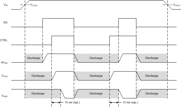
The device discharges outputs during shutdown. Figure 7 shows the discharge control.
 Figure 7. Outputs Discharge During Shut Down
8.3.9 Thermal Shutdown
The TPS65632 device enters thermal shutdown if its junction temperature exceeds 145°C (typical). During thermal shutdown none of the device's functions are available. To resume normal operation VI has to cycle below the undervoltage threshold, or CTRL has to toggle LOW and then HIGH.
8.4 Device Functional Modes
8.4.1 Operation with VI < 2.9 V
The recommended minimum input supply voltage for full-performance is 2.9 V. The device continues to operate with input supply voltages below 2.9 V, however, full performance is not guaranteed. The TPS65632 device does not operate with input supply voltages below the UVLO threshold.
8.4.2 Operation with VI ≈ VPOS (Diode Mode)
The TPS65632 device features a "diode" mode that enables it to regulate its VPOS output even when the input supply voltage is close to VPOS (that is, too high for normal boost operation). When operating in diode mode the VPOS boost converter's high-side switch is disabled and its body diode used as the rectifier. Note that a minimum load of ≈2 mA is required to proper output regulation in diode mode.
8.4.3 Operation with CTRL
When a low-level signal is applied to the CTRL pin the device is disabled and switching is inhibited. When the input supply voltage is above the UVLO threshold and a high-level signal is applied to the CTRL pin the device is enabled and its start-up sequence begins.