ZHCSBX0C december 2013 – may 2023 TPS65261 , TPS65261-1
PRODUCTION DATA
- 1
- 1 特性
- 2 应用
- 3 说明
- 4 Revision History
- 5 Pin Configuration and Functions
- 6 Specifications
-
7 Detailed Description
- 7.1 Overview
- 7.2 Functional Block Diagram
- 7.3
Feature Description
- 7.3.1 Adjusting the Output Voltage
- 7.3.2 Power Failure Detector
- 7.3.3 Enable and Adjusting Undervoltage Lockout
- 7.3.4 Soft-Start Time
- 7.3.5 Power Up Sequencing
- 7.3.6 V7V Low Dropout Regulator and Bootstrap
- 7.3.7 Out-of-Phase Operation
- 7.3.8 Output Overvoltage Protection (OVP)
- 7.3.9 Slope Compensation
- 7.3.10 Overcurrent Protection
- 7.3.11 Power Good
- 7.3.12 Adjustable Switching Frequency
- 7.3.13 Thermal Shutdown
- 7.4 Device Functional Modes
- 8 Application and Implementation
- 9 Device and Documentation Support
- 10Mechanical, Packaging, and Orderable Information
7.3.4 Soft-Start Time
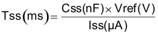
The voltage on the respective SS pin controls the start-up of the buck output. When the voltage on the SS pin is less than the internal 0.6V reference, the TPS65261, TPS65261-1 regulates the internal feedback voltage to the voltage on the SS pin instead of 0.6V. The SS pin can be used to program an external soft-start function or to allow output of the buck to track another supply during start-up. The device has an internal pull-up current source of 5µA (typical) that charges an external soft-start capacitor to provide a linear ramping voltage at the SS pin. The TPS65261, TPS65261-1 regulates the internal feedback voltage to the voltage on the SS pin, allowing VOUT to rise smoothly from 0V to its regulated voltage without inrush current. The soft-start time can be calculated approximately by Equation 8.
Many of the common power supply sequencing methods can be implemented using the SSx and ENx pins. Figure 7-6 shows the method implementing ratio-metric sequencing by connecting the SSx pins of three buck channels together. The regulator outputs ramp up and reach regulation at the same time. When calculating the soft-start time, the pull-up current source must be tripled in Equation 8.
 Figure 7-6 Ratio Metric Power Up Using SSx Pins
Simultaneous power supply sequencing can be implemented by connecting capacitor to SSx pin, shown in Figure 7-7. The capacitors can be calculated using Equation 8 and Equation 9.
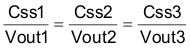
 Figure 7-7 Simultaneous Startup Sequence Using SSx Pins