SLVS754D March 2007 – January 2015 TPS65053
PRODUCTION DATA.
- 1 Features
- 2 Applications
- 3 Description
- 4 Revision History
- 5 Pin Configuration and Functions
- 6 Specifications
-
7 Detailed Description
- 7.1 Overview
- 7.2 Functional Block Diagrams
- 7.3 Feature Description
- 7.4 Device Functional Modes
-
8 Application and Implementation
- 8.1 Application Information
- 8.2
Typical Application
- 8.2.1 Design Requirements
- 8.2.2 Detailed Design Procedure
- 8.2.3 Application Curves
- 9 Power Supply Recommendations
- 10Layout
- 11Device and Documentation Support
- 12Mechanical, Packaging, and Orderable Information
8 Application and Implementation
NOTE
Information in the following applications sections is not part of the TI component specification, and TI does not warrant its accuracy or completeness. TI’s customers are responsible for determining suitability of components for their purposes. Customers should validate and test their design implementation to confirm system functionality.
8.1 Application Information
This device integrates two step-down converters and three LDOs which can be used to power the voltage rails needed by a processor or any other application. The PMIC can be controlled via the ENABLE and MODE pins or sequenced from the VIN using RC delay circuits. There is a logic output, RESET, provide the application processor or load a logic signal indicating power good or reset.
8.2 Typical Application
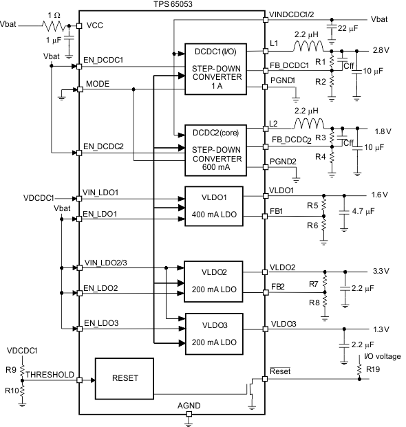 Figure 25. Typical Application Schematic
8.2.1 Design Requirements
The TPS6505x has only a few design requirements. The check list below lists the design requirements across all application uses of the device.
- 1-µF Bypass cap on VCC, located as close as possible to the VCC pin to ground.
- VCC and VINDCDC1/2 must be connected to the same voltage supply with minimal voltage difference.
- Input capacitors must be present on the VINDCDC1/2, VIN_LDO1, and VIN_LDO2/3 supplies if used.
- Output filters must be used on the outputs of the DCDC converters if used.
- Output capacitors must be used on the outputs of the LDOs if used.
8.2.2 Detailed Design Procedure
The TPS6505x requires design for each regulator whether DCDC or LDO. First, the output votlage must be selected or set. Then, each DCDC converter requires an output filter, input capacitor, and feedback circuit and each LDO requires an output capacitor and input capacitor. The following sections discuss the procedure for designing for output voltages, DCDCs, and LDOs.
8.2.2.1 DCDC Output Voltage Setting
The output voltage of the DCDC converters can be set by an external resistor network and can be calculated to:

with an internal reference voltage Vref, 0.6 V (typical).
It is recommended to set the total resistance of R1 + R2 to less than 1 MΩ. The resistor network connects to the input of the feedback amplifier; therefore, need some small feedforward capacitor in parallel to R1. A typical value of 47 pF is sufficient.
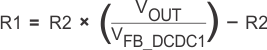
Table 3. Typical Resistor Values
| OUTPUT VOLTAGE | R1 | R2 | NOMINAL VOLTAGE | TYPICAL CFF |
|---|---|---|---|---|
| 3.3 V | 680 kΩ | 150 kΩ | 3.32 V | 47 pF |
| 3.0 V | 510 kΩ | 130 kΩ | 2.95 V | 47 pF |
| 2.85 V | 560 kΩ | 150 kΩ | 2.84 V | 47 pF |
| 2.5 V | 510 kΩ | 160 kΩ | 2.51 V | 47 pF |
| 1.8 V | 300 kΩ | 150 kΩ | 1.80 V | 47 pF |
| 1.6 V | 200 kΩ | 120 kΩ | 1.60 V | 47 pF |
| 1.5 V | 300 kΩ | 200 kΩ | 1.50 V | 47 pF |
| 1.2 V | 330 kΩ | 330 kΩ | 1.20 V | 47 pF |
8.2.2.2 LDO Output Voltage Setting
The output voltage of LDO1 and LDO2 can be set by an external resistor network and can be calculated to:

with an internal reference voltage, VREF, typical 1 V.
It is recommended to set the total resistance of R5 + R6 to less than 1 MΩ. Typically, there is no feedforward capacitor needed at the voltage dividers for the LDOs.

Table 4. Typical Resistor Values
| OUTPUT VOLTAGE | R5 | R6 | NOMINAL VOLTAGE |
|---|---|---|---|
| 3.3 V | 300 kΩ | 130 kΩ | 3.31 V |
| 3 V | 300 kΩ | 150 kΩ | 3.00 V |
| 2.85 V | 240 kΩ | 130 kΩ | 2.85 V |
| 2.80 V | 360 kΩ | 200 kΩ | 2.80 V |
| 2.5 V | 300 kΩ | 200 kΩ | 2.50 V |
| 1.8 V | 240 kΩ | 300 kΩ | 1.80 V |
| 1.5 V | 150 kΩ | 300 kΩ | 1.50 V |
| 1.3 V | 36 kΩ | 120 kΩ | 1.30 V |
| 1.2 V | 100 kΩ | 510 kΩ | 1.19 V |
| 1.1 V | 33 kΩ | 330 kΩ | 1.1 V |
8.2.2.3 Low Dropout Voltage Regulators
The low dropout voltage regulators are designed to be stable with low value ceramic input and output capacitors. They operate with input voltages down to 1.5 V. The LDOs offer a maximum dropout voltage of 280mV at rated output current. Each LDO supports a current limit feature. The LDOs are enabled by the EN_LDO1, EN_LDO2, and EN_LDO3 pin. The output voltage of LDO1 and LDO2 is set using an external resistor divider whereas LDO3 has a fixed output voltage of 1.30 V for TPS65053, 1.20 V for TPS650531 and 1.50 V for TPS650532.
The minimum input capacitor on VIN_LDO1 and on VIN_LDO2/3 is 2.2 μF minimum. LDO1 is designed to be stable with an output capacitor of 4.7 μF minimum; whereas, LDO2 and LDO3 are stable with a minimum capacitor value of 2.2 μF.
8.2.2.4 DCDC Output Filter Design (Inductor and Output Capacitor)
8.2.2.4.1 Inductor Selection
The two converters operate typically with 2.2-μH output inductor. Larger or smaller inductor values can be used to optimize the performance of the device for specific operation conditions. For output voltages higher than 2.8 V, an inductor value of 3.3 μH minimum should be selected, otherwise the inductor current will ramp down too fast causing imprecise internal current measurement and therefore increased output voltage ripple under some operating conditions in PFM mode.
The selected inductor has to be rated for its DC resistance and saturation current. The DC resistance of the inductance will influence directly the efficiency of the converter. Therefore an inductor with lowest DC resistance should be selected for highest efficiency.
Equation 8 calculates the maximum inductor current under static load conditions. The saturation current of the inductor should be rated higher than the maximum inductor current as calculated with Equation 8. This is recommended because during heavy load transient the inductor current will rise above the calculated value.
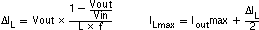
where
- f = Switching Frequency (2.25-MHz typical)
- L = Inductor Value
- Δ IL = Peak-to-peak inductor ripple current
- ILmax = Maximum Inductor current
The highest inductor current occurs at maximum Vin. Open core inductors have a soft saturation characteristic, and they can normally handle higher inductor currents versus a comparable shielded inductor.
A more conservative approach is to select the inductor current rating just for the maximum switch current of the corresponding converter. It must be considered, that the core material from inductor to inductor differs and will have an impact on the efficiency especially at high switching frequencies. Refer to Table 5 and the typical applications for possible inductors.
Table 5. Tested Inductors
| INDUCTOR TYPE | INDUCTOR VALUE | SUPPLIER |
|---|---|---|
| LPS3010 | 2.2 μH | Coilcraft |
| LPS3015 | 3.3 μH | Coilcraft |
| LPS4012 | 2.2 μH | Coilcraft |
| VLF4012 | 2.2 μH | TDK |
8.2.2.4.2 Output Capacitor Selection
The advanced Fast Response voltage mode control scheme of the two converters allow the use of small ceramic capacitors with a typical value of 10 μF, without having large output voltage under and overshoots during heavy load transients. Ceramic capacitors having low ESR values result in lowest output voltage ripple and are therefore recommended. See the recommended components in Table 4.
If ceramic output capacitors are used, the capacitor RMS ripple current rating will always meet the application requirements. Just for completeness, the RMS ripple current is calculated as:
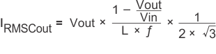
At nominal load current, the inductive converters operate in PWM mode and the overall output voltage ripple is the sum of the voltage spike caused by the output capacitor ESR plus the voltage ripple caused by charging and discharging the output capacitor:
Where the highest output voltage ripple occurs at the highest input voltage Vin.
At light load currents, the converters operate in Power Save Mode and the output voltage ripple is dependent on the output capacitor value. The output voltage ripple is set by the internal comparator delay and the external capacitor. The typical output voltage ripple is less than 1% of the nominal output voltage.
8.2.2.5 DCDC Input Capacitor Selection
Because of the nature of the buck converter, having a pulsating input current, a low ESR input capacitor is required for best input voltage filtering and minimizing the interference with other circuits caused by high input voltage spikes. The converters need a ceramic input capacitor of 10 μF. The input capacitor can be increased without any limit for better input voltage filtering.
Table 6. Possible Capacitors For DCDC Converters and LDOS
| CAPACITOR VALUE | SIZE | SUPPLIER | TYPE |
|---|---|---|---|
| 2.2 μF | 0805 | TDK C2012X5R0J226MT | Ceramic |
| 2.2 μF | 0805 | Taiyo Yuden JMK212BJ226MG | Ceramic |
| 10 μF | 0805 | Taiyo Yuden JMK212BJ106M | Ceramic |
| 10 μF | 0805 | TDK C2012X5R0J106M | Ceramic |
8.2.2.6 Sequencing and Output Logic Signal RESET
To sequence the TPS6505x, the regulators can be sequenced by using the enable pins on each DCDC and LDO. A sequencer could be used but, simply looping back the output voltages of the preceeding rail to the enable input of the following rail can sequence the PMIC with minimal cost and solution area. Simple and small RC delay circuits could be added to create timing delays for enabling if needed.
Use the THRESHOLD and RESET feature to provide a logic signal to the application or processor. THRESHOLD requires a voltage divider if the signal being monitored is desired to trigger RESET at a point higher than 1V.
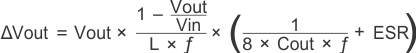
8.2.3 Application Curves
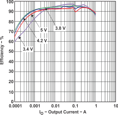 Figure 26. Efficiency Converter 1 on TPS65053
 Figure 27. Efficiency Converter 2 on TPS65053