ZHCSIG5E July 2018 – August 2021 TPS63805 , TPS63806 , TPS63807
PRODUCTION DATA
- 1 特性
- 2 应用
- 3 说明
- 4 Revision History
- 5 说明(续)
- 6 Device Comparison Table
- 7 Pin Configuration and Functions
- 8 Specifications
-
9 Detailed Description
- 9.1 Overview
- 9.2 Functional Block Diagram
- 9.3
Feature Description
- 9.3.1 Control Loop Description
- 9.3.2 Precise Device Enable: Threshold- or Delayed Enable
- 9.3.3 Mode Selection (PFM/PWM)
- 9.3.4 Undervoltage Lockout (UVLO)
- 9.3.5 Soft Start
- 9.3.6 Adjustable Output Voltage
- 9.3.7 Overtemperature Protection - Thermal Shutdown
- 9.3.8 Input Overvoltage - Reverse-Boost Protection (IVP)
- 9.3.9 Output Overvoltage Protection (OVP)
- 9.3.10 Power-Good Indicator
- 9.4 Device Functional Modes
- 10Application and Implementation
- 11Power Supply Recommendations
- 12Layout
- 13Device and Documentation Support
- 14Mechanical, Packaging, and Orderable Information
9.3.1 Control Loop Description
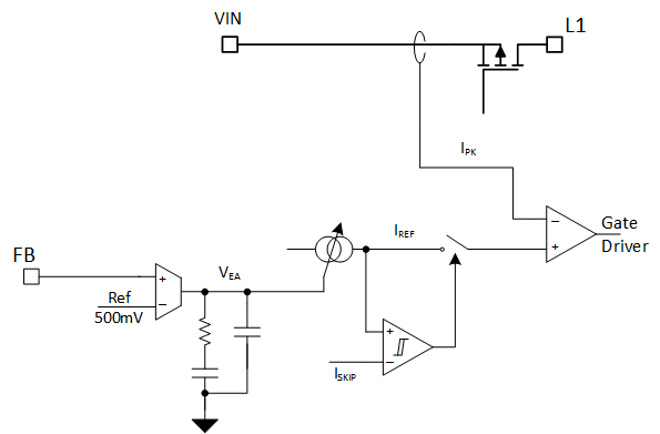
The TPS63805, TPS63806, and TPS63807 use a peak current mode control architecture. It has an inner current loop where it measures the peak current of the boost high-side MOSFET and compares it to a reference current. This current is the output of the outer voltage loop. It measures the output voltage via the FB-pin and compares it with the internal voltage reference. That means, the outer voltage loop measures the voltage error (VREF-VFB), and transforms it into the system current demand (IREF) for the inner current loop.
Figure 9-1 shows the simplified schematic of the control loop. The error amplifier and the type-2 compensation represent the voltage loop. The voltage output is converted into the reference current IREF and fed into the current comparator.
The scheme shows the skip-comparator handling the power-save mode (PFM) to achieve high efficiency at light loads. See Section 9.4.2 for further details.
 Figure 9-1 Control Loop Architecture Scheme