ZHCSDM2A November 2014 – December 2014 TPS63024 , TPS630241 , TPS630242
PRODUCTION DATA.
- 1 特性
- 2 应用范围
- 3 说明
- 4 修订历史记录
- 5 Pin Configuration and Functions
- 6 Specifications
- 7 Detailed Description
- 8 Application and Implementation
- 9 Power Supply Recommendations
- 10Layout
- 11器件和文档支持
- 12机械、封装和可订购信息
6 Specifications
6.1 Absolute Maximum Ratings(4)
over junction temperature range (unless otherwise noted)| VALUE | ||||
|---|---|---|---|---|
| MIN | MAX | UNIT | ||
| Voltage(1) | VIN, L1, EN, VINA, PFM/PWM | –0.3 | 7 | V |
| VOUT, FB | –0.3 | 4 | V | |
| L2(2) | –0.3 | 4 | V | |
| L2(3) | -0.3 | 5.5 | V | |
| Input current | Continuos average current into L1(5) | 2.7 | A | |
| TJ | Operating junction temperature | –40 | 125 | °C |
| Tstg | Storage temperature range | –65 | 150 | |
(1) All voltage values are with respect to network ground pin.
(2) DC voltage rating.
(3) AC transient voltage rating.
(4) Stresses beyond those listed under Absolute Maximum Ratings may cause permanent damage to the device. These are stress ratings only, which do not imply functional operation of the device at these or any other conditions beyond those indicated under Recommended Operating Conditions. Exposure to absolute-maximum-rated conditions for extended periods may affect device reliability.
(5) Maximum continuos average input current 3.5A, under those condition do not exceed 105°C for more than 25% operating time.
6.2 ESD Ratings
| VALUE | UNIT | |||
|---|---|---|---|---|
| V(ESD) | Electrostatic discharge | Human-body model (HBM), per ANSI/ESDA/JEDEC JS-001(1) | ±2000 | V |
| Charged-device model (CDM), per JEDEC specification JESD22-C101(2) | ±700 | |||
(1) JEDEC document JEP155 states that 500-V HBM allows safe manufacturing with a standard ESD control process.
(2) JEDEC document JEP157 states that 250-V CDM allows safe manufacturing with a standard ESD control process.
6.3 Recommended Operating Conditions(1)
| MIN | TYP | MAX | UNIT | ||
|---|---|---|---|---|---|
| VIN | Input Voltage Range | 2.3 | 5.5 | V | |
| VOUT | Output Voltage | 2.5 | 3.6 | V | |
| L | Inductance (3) | 0.5 | 1 | 1.3 | µH |
| Cout | Output Capacitance(2) | 16 | µF | ||
| TA | Operating ambient temperature | –40 | 85 | °C | |
| TJ | Operating virtual junction temperature | –40 | 125 | °C |
(1) Refer to the Application Information section for further information
(2) Due to the dc bias effect of ceramic capacitors, the effective capacitance is lower then the nominal value when a voltage is applied. This is why the capacitance is specified to allow the selection of the nominal capacitor required with the dc bias effect for this type of capacitor. The nominal value given matches a typical capacitor to be chosen to meet the minimum capacitance required.
(3) Effective inductance value at operating condition. The nominal value given matches a typical inductor to be chosen to meet the inductance required.
6.4 Thermal Information
| THERMAL METRIC(1) | TPS63024x | UNIT | |
|---|---|---|---|
| YFF | |||
| 20 PINS | |||
| RθJA | Junction-to-ambient thermal resistance | 53.8 | °C/W |
| RθJC(top) | Junction-to-case (top) thermal resistance | 0.5 | |
| RθJB | Junction-to-board thermal resistance | 10.1 | |
| ψJT | Junction-to-top characterization parameter | 1.4 | |
| ψJB | Junction-to-board characterization parameter | 9.8 | |
| RθJC(bot) | Junction-to-case (bottom) thermal resistance | N/A | |
(1) For more information about traditional and new thermal metrics, see the IC Package Thermal Metrics application report, SPRA953.
6.5 Electrical Characteristics
VIN=2.3V to 5.5V, TJ= –40°C to 125°C, typical values are at TA=25°C (unless otherwise noted)| PARAMETER | TEST CONDITIONS | MIN | TYP | MAX | UNIT | |||
|---|---|---|---|---|---|---|---|---|
| SUPPLY | ||||||||
| VIN | Input voltage range | 2.3 | 5.5 | V | ||||
| VIN_Min | Minimum input voltage to turn on into full load | RLOAD= 2.2Ω | 2.7 | V | ||||
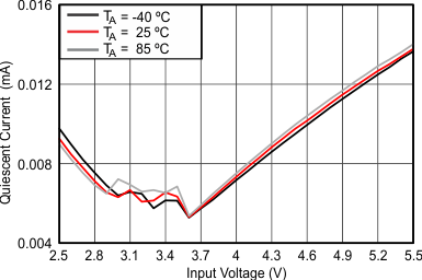
| IQ | Quiescent current | VIN | IOUT=0mA, EN=VIN=3.6V, VOUT=3.3V TJ=-40°C to 85°C, not switching | 35 | 70 | μA | ||
| VOUT | 12 | μA | ||||||
| Isd | Shutdown current | EN=low, TJ=-40°C to 85°C | 0.1 | 2 | μA | |||
| UVLO | Under voltage lockout threshold | VIN falling | 1.6 | 1.7 | 2 | V | ||
| Under voltage lockout hysteresis | 70 | mV | ||||||
| Thermal shutdown | Temperature rising | 140 | °C | |||||
| LOGIC SIGNALS EN, PFM/PWM | ||||||||
| VIH | High level input voltage | VIN=2.3V to 5.5V | 1.2 | V | ||||
| VIL | Low level input voltage | VIN=2.3V to 5.5V | 0.4 | V | ||||
| Ilkg | Input leakage current | PFM/PWM, EN=GND or VIN | 0.01 | 0.2 | μA | |||
| OUTPUT | ||||||||
| VOUT | Output Voltage range | 2.5 | 3.6 | V | ||||
| VFB | Feedback regulation voltage | TPS63024 | 0.8 | V | ||||
| VFB | Feedback voltage accuracy | PWM mode, TPS63024 | -1% | 1% | ||||
| VFB | Feedback voltage accuracy (2) | PFM mode, TPS63024 | -1% | 1.3% | +3% | |||
| VOUT | Output voltage accuracy | PWM mode, TPS630241 | 2.871 | 2.9 | 2.929 | V | ||
| VOUT | Output voltage accuracy(2) | PFM mode, TPS630241 | 2.871 | 2.938 | 2.987 | V | ||
| VOUT | Output voltage accuracy | PWM mode, TPS630242 | 3.267 | 3.3 | 3.333 | V | ||
| VOUT | Output voltage accuracy(2) | PFM mode, TPS630242 | 3.267 | 3.343 | 3.399 | V | ||
| IPWM/PFM | Output current to enter PFM mode | VIN =3V; VOUT = 3.3V | 350 | mA | ||||
| IFB | Feedback input bias current | VFB = 0.8V | 10 | 100 | nA | |||
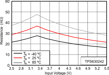
| RDS_Buck(on) | High side FET on-resistance | VIN=3.0V, VOUT=3.3V | 35 | mΩ | ||||
| Low side FET on-resistance | VIN=3.0V, VOUT=3.3V | 50 | mΩ | |||||
| RDS_Boost(on) | High side FET on-resistance | VIN=3.0V, VOUT=3.3V | 25 | mΩ | ||||
| Low side FET on-resistance | VIN=3.0V, VOUT=3.3V | 50 | mΩ | |||||
| IIN | Average input current limit (1) | VIN=3.0V, VOUT=3.3V TJ= 25°C to 125°C | 2.12 | 3 | 3.54 | A | ||
| fs | Switching Frequency | 2.5 | MHz | |||||
| RON_DISC | Discharge ON-Resistance | EN=low | 120 | Ω | ||||
| Line regulation | VIN=2.8V to 5.5V, IOUT=1.5A | 7.4 | mV/V | |||||
| Load regulation | VIN=3.6V,IOUT=0A to 1.5A | 2.5 | mV/A | |||||
(1) For variation of this parameter with Input voltage and temperature see Figure 8. To calculate minimum output current in a specific working point see Figure 8 and Equation 1 trough Equation 4.
(2) Conditions: L=1 µH, COUT= 2 × 22µF.
6.6 Timing Requirements
VIN= 2.3V to 5.5V, TJ= –40°C to 125°C, typical values are at TA= 25°C (unless otherwise noted)| PARAMETER | TEST CONDITIONS | MIN | TYP | MAX | UNIT | |||
|---|---|---|---|---|---|---|---|---|
| OUTPUT | ||||||||
| tSS | Softstart time | EN=low to high, Buck mode VIN=3.6V, VOUT=3.3V, IOUT=1.5A | 450 | µs | ||||
| EN=low to high, Boost mode VIN=2.8V, VOUT=3.3V, IOUT=1.5A | 700 | µs | ||||||
| td | Start up delay | Time from when EN=high to when device starts switching | 100 | µs | ||||
6.7 Typical Characteristics
.
.

