SLVS871D February 2010 – June 2016 TPS62660 , TPS62665
PRODUCTION DATA.
- 1 Features
- 2 Applications
- 3 Description
- 4 Revision History
- 5 Pin Configuration and Functions
- 6 Specifications
- 7 Parameter Measurement Information
- 8 Detailed Description
- 9 Application and Implementation
- 10Power Supply Recommendations
- 11Layout
- 12Device and Documentation Support
- 13Mechanical, Packaging, and Orderable Information
6 Specifications
6.1 Absolute Maximum Ratings
over operating free-air temperature range (unless otherwise noted)(1)| MIN | MAX | UNIT | ||
|---|---|---|---|---|
| VI | Voltage at VIN, SW(2) | –0.3 | 7 | V |
| Voltage at FB(2) | –0.3 | 3.6 | V | |
| Voltage at EN, MODE (2) | –0.3 | VI + 0.3 | V | |
| IO | Peak output current | 1000 | mA | |
| Power dissipation | Internally limited | |||
| TA | Operating temperature(3) | –40 | 85 | °C |
| TJ (max) | Maximum operating junction temperature | 150 | °C | |
| Tstg | Storage temperature | –65 | 150 | °C |
(1) Stresses beyond those listed under Absolute Maximum Ratings may cause permanent damage to the device. These are stress ratings only and functional operation of the device at these or any other conditions beyond those indicated under Recommended Operating Conditions is not implied. Exposure to absolute-maximum-rated conditions for extended periods may affect device reliability.
(2) All voltage values are with respect to network ground terminal.
(3) In applications where high power dissipation and/or poor package thermal resistance is present, the maximum ambient temperature may have to be derated. Maximum ambient temperature (TA(max)) is dependent on the maximum operating junction temperature (TJ(max)), the maximum power dissipation of the device in the application (PD(max)), and the junction-to-ambient thermal resistance of the part/package in the application (RθJA), as given by the following equation: TA(max)= TJ(max) – (RθJA × PD(max)). To achieve optimum performance, it is recommended to operate the device with a maximum junction temperature of 105°C.
6.2 ESD Ratings
| VALUE | UNIT | |||
|---|---|---|---|---|
| V(ESD) | Electrostatic discharge(1) | Human-body model (HBM), per ANSI/ESDA/JEDEC JS-001(2) | ±2000 | V |
| Charged-device model (CDM), per JEDEC specification JESD22-C101(3) | ±1000 | |||
| Machine model (MM) | ±200 | |||
(1) The human-body model is a 100-pF capacitor discharged through a 1.5-kΩ resistor into each pin. The machine model is a 200-pF capacitor discharged directly into each pin.
(2) JEDEC document JEP155 states that 500-V HBM allows safe manufacturing with a standard ESD control process.
(3) JEDEC document JEP157 states that 250-V CDM allows safe manufacturing with a standard ESD control process.
6.3 Recommended Operating Conditions
over operating free-air temperature range (unless otherwise noted)| MIN | NOM | MAX | UNIT | ||
|---|---|---|---|---|---|
| VI | Supply voltage | 2.3 | 5.5 | V | |
| IOUT | Maximum output current | 1000 | mA | ||
| Effective inductance | 0.3 | 0.47 | 1.3 | µH | |
| TA | Operating ambient temperature | –40 | 85 | °C | |
| TJ | Operating junction temperature | –40 | 125 | °C | |
6.4 Thermal Information
| THERMAL METRIC(1) | TPS626xx | UNIT | |
|---|---|---|---|
| YFF (DSBGA) | |||
| 6 PINS | |||
| RθJA | Junction-to-ambient thermal resistance | 130 | °C/W |
| RθJC(top) | Junction-to-case (top) thermal resistance | 1.2 | °C/W |
| RθJB | Junction-to-board thermal resistance | 22 | °C/W |
| ψJT | Junction-to-top characterization parameter | 5 | °C/W |
| ψJB | Junction-to-board characterization parameter | 22 | °C/W |
| RθJC(bot) | Junction-to-case (bottom) thermal resistance | N/A | °C/W |
(1) For more information about traditional and new thermal metrics, see the Semiconductor and IC Package Thermal Metrics application report.
6.5 Electrical Characteristics
Minimum and maximum values are at VI = 2.3 V to 5.5 V, VO = 1.8 V, EN = 1.8 V, AUTO mode and TA = –40°C to 85°C; circuit in the Parameter Measurement Information (unless otherwise noted). Typical values are at VI = 3.6 V, VO = 1.8 V, EN = 1.8 V, AUTO mode and TA = 25°C (unless otherwise noted).6.6 Dissipation Ratings(1)
| PACKAGE | RθJA (2) | RθJB (2) | POWER RATING TA ≤ 25°C |
DERATING FACTOR ABOVE TA = 25°C |
|---|---|---|---|---|
| YFF-6 | 125°C/W | 53°C/W | 800 mW | 8 mW/°C |
(1) Maximum power dissipation is a function of TJ(max), RθJA, and TA. The maximum allowable power dissipation at any allowable ambient temperature is PD = [TJ(max)-TA] / RθJA.
(2) This thermal data is measured with high-K board (4-layer board according to JESD51-7 JEDEC standard).
6.7 Typical Characteristics
Table 1. Table of Graphs
| FIGURE | |||
|---|---|---|---|
| η | Efficiency | vs load current | Figure 1, Figure 2, Figure 3, Figure 4 |
| vs input voltage | Figure 5 | ||
| Peak-to-peak output ripple current | vs load current | Figure 6, Figure 7 | |
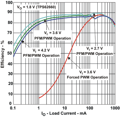 Figure 1. Efficiency vs Load Current
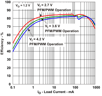 Figure 3. Efficiency vs Load Current
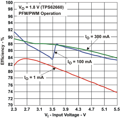 Figure 5. Efficiency vs Input Voltage
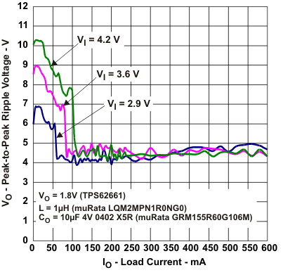 Figure 7. Peak-to-Peak Output Ripple Voltage vs Load Current
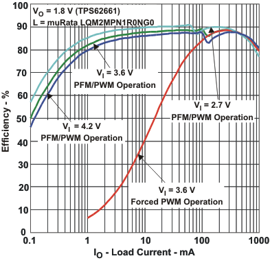 Figure 2. Efficiency vs Load Current
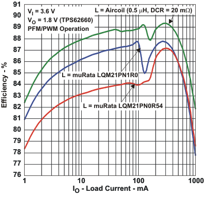 Figure 4. Efficiency vs Load Current
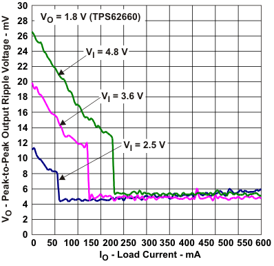 Figure 6. Peak-to-Peak Output Ripple Voltage vs Load Current