ZHCSB86E November   2011  – October 2021 TPS62150 , TPS62150A , TPS62151 , TPS62152 , TPS62153

PRODUCTION DATA  

  1. 特性
  2. 应用
  3. 说明
  4. Revision History
  5. Device Comparison Table
  6. Pin Configuration and Functions
  7. Specifications
    1. 7.1 Absolute Maximum Ratings (1)
    2. 7.2 ESD Ratings
    3. 7.3 Recommended Operating Conditions
    4. 7.4 Thermal Information
    5. 7.5 Electrical Characteristics
    6. 7.6 Typical Characteristics
  8. Detailed Description
    1. 8.1 Overview
    2. 8.2 Functional Block Diagrams
    3. 8.3 Feature Description
      1. 8.3.1 Enable / Shutdown (EN)
      2. 8.3.2 Soft Start or Tracking (SS/TR)
      3. 8.3.3 Power Good (PG)
      4. 8.3.4 Pin-Selectable Output Voltage (DEF)
      5. 8.3.5 Frequency Selection (FSW)
      6. 8.3.6 Undervoltage Lockout (UVLO)
      7. 8.3.7 Thermal Shutdown
    4. 8.4 Device Functional Modes
      1. 8.4.1 Pulse-Width Modulation (PWM) Operation
      2. 8.4.2 Power-Save Mode Operation
      3. 8.4.3 100% Duty-Cycle Operation
      4. 8.4.4 Current-Limit and Short-Circuit Protection
  9. Application and Implementation
    1. 9.1 Application Information
    2. 9.2 Typical Application
      1. 9.2.1 Design Requirements
      2. 9.2.2 Detailed Design Procedure
        1. 9.2.2.1 Programming the Output Voltage
        2. 9.2.2.2 External Component Selection
          1. 9.2.2.2.1 Inductor Selection
          2. 9.2.2.2.2 Capacitor Selection
            1. 9.2.2.2.2.1 Output Capacitor
            2. 9.2.2.2.2.2 Input Capacitor
            3. 9.2.2.2.2.3 Soft-Start Capacitor
        3. 9.2.2.3 Tracking Function
        4. 9.2.2.4 Output Filter and Loop Stability
      3. 9.2.3 Application Curves
    3. 9.3 System Examples
      1. 9.3.1 LED Power Supply
      2. 9.3.2 Active Output Discharge
      3. 9.3.3 Inverting Power Supply
      4. 9.3.4 Various Output Voltages
  10. 10Power Supply Recommendations
  11. 11Layout
    1. 11.1 Layout Guidelines
    2. 11.2 Layout Example
      1. 11.2.1 Thermal Considerations
  12. 12Device and Documentation Support
    1. 12.1 Device Support
      1. 12.1.1 第三方产品免责声明
    2. 12.2 Documentation Support
      1. 12.2.1 Related Documentation
    3. 12.3 接收文档更新通知
    4. 12.4 支持资源
    5. 12.5 Trademarks
    6. 12.6 Electrostatic Discharge Caution
    7. 12.7 术语表
  13. 13Mechanical, Packaging, and Orderable Information

封装选项

机械数据 (封装 | 引脚)
散热焊盘机械数据 (封装 | 引脚)
订购信息

Power-Save Mode Operation

The TPS6215x enters its built-in power-save mode seamlessly if the load current decreases. This secures a high efficiency in light load operation. The device remains in power-save mode as long as the inductor current is discontinuous.

In power-save mode, the switching frequency decreases linearly with the load current, maintaining high efficiency. The transition into and out of power-save mode happens within the entire regulation scheme and is seamless in both directions.

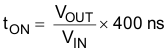
TPS6215x includes a fixed on-time circuitry. An estimate for this on-time, in steady-state operation with FSW = low, is:

Equation 1. GUID-BC989441-0938-4202-8024-0D47FEAE8466-low.gif

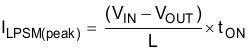
For very small output voltages, an absolute minimum on-time of about 80 ns is kept to limit switching losses. The operating frequency is thereby reduced from its nominal value, which keeps efficiency high. Also, the off-time can reach its minimum value at high duty cycles. The output voltage remains regulated in such cases. Using tON, the typical peak inductor current in power-save mode is approximated by:

Equation 2. GUID-88B96866-86A9-4178-A33B-B1442EC0E70D-low.gif

When VIN decreases to typically 15% above VOUT, the TPS62150x device does not enter power-save mode, regardless of the load current. The device maintains output regulation in PWM mode.