SLVSDV2 March 2017 TPS62136
PRODUCTION DATA.
- 1 Features
- 2 Applications
- 3 Description
- 4 Revision History
- 5 Device Comparison Table
- 6 Pin Configuration and Functions
- 7 Specifications
- 8 Parameter Measurement Information
-
9 Detailed Description
- 9.1 Overview
- 9.2 Functional Block Diagram
- 9.3 Feature Description
- 9.4
Device Functional Modes
- 9.4.1 Pulse Width Modulation (PWM) Operation
- 9.4.2 Power Save Mode Operation (PWM/PFM)
- 9.4.3 100% Duty-Cycle Operation
- 9.4.4 HICCUP Current Limit And Short Circuit Protection (TPS62136 only)
- 9.4.5 Current Limit And Short Circuit Protection (TPS621361 only)
- 9.4.6 Soft-Start / Tracking (SS/TR)
- 9.4.7 Output Discharge Function (TPS62136 only)
- 9.4.8 Starting into a Pre-Biased Load (TPS621361 only)
- 10Application and Implementation
- 11Power Supply Recommendations
- 12Layout
- 13Device and Documentation Support
- 14Mechanical, Packaging, and Orderable Information
10 Application and Implementation
NOTE
Information in the following applications sections is not part of the TI component specification, and TI does not warrant its accuracy or completeness. TI’s customers are responsible for determining suitability of components for their purposes. Customers should validate and test their design implementation to confirm system functionality.
10.1 Application Information
10.1.1 Programming the Output Voltage
The output voltage of the TPS62136x is adjustable. It can be programmed for output voltages from 0.8 V to 12 V, using a resistor divider from VOUT to GND. The voltage at the FB pin is regulated to 700 mV. The value of the output voltage is set by the selection of the resistor divider from Equation 8. It is recommended to choose resistor values which allow a current of at least 2 uA, meaning the value of R2 should not exceed 400 kΩ. Lower resistor values are recommended for highest accuracy and most robust design.

10.1.2 External Component Selection
The external components have to fulfill the needs of the application, but also the stability criteria of the device´s control loop. The TPS62136x is optimized to work within a range of external components. The LC output filters inductance and capacitance have to be considered together, creating a double pole, responsible for the corner frequency of the converter (see Output Filter and Loop Stability). Table 2 can be used to simplify the output filter component selection.
Table 2. Recommended LC Output Filter Combinations(1)
| 10 µF | 22 µF | 47 µF | 68 µF | 100 µF | 200 µF | ≥400 µF | |
|---|---|---|---|---|---|---|---|
| 1.0 µH | |||||||
| 1.5 µH | √(2) | √ | √ | √ | √(3) | ||
| 2.2 µH | √ | √ | √ | √ | √(3) | ||
| 3.3 µH |
10.1.3 Inductor Selection
The TPS62136x is designed for a nominal 1.5-µH or 2.2-µH inductor. Please see the recommended operating conditions for the range of inductance. Smaller values than 1.5µH will cause a larger inductor current ripple which causes larger negative inductor current in forced PWM mode at low or no output current. Therefore they are not recommended at large voltages across the inductor as it is the case for high input voltages and low output voltages. With low output current in forced PWM mode this causes a larger negative inductor current peak which may exceed the negative current limit. At low or no output current and small inductor values the output voltage can therefore not be regulated any more.
The inductor selection is affected by several effects like inductor ripple current, output ripple voltage, PWM-to-PFM transition point and efficiency. In addition, the inductor selected has to be rated for appropriate saturation current and DC resistance (DCR). Equation 9 calculates the maximum inductor current.


where:
IL(max) is the maximum inductor current
ΔIL is the Peak to Peak Inductor Ripple Current
L(min) is the minimum effective inductor value.
Calculating the maximum inductor current using the actual operating conditions gives the minimum saturation current of the inductor needed. A margin of about 20% is recommended to add. A larger inductor value is also useful to get lower ripple current, but increases the transient response time and size as well. The following inductors have been used with the TPS62136x and are recommended for use:
Table 3. List of Inductors
| TYPE | INDUCTANCE [µH] | CURRENT [A](1) | DIMENSIONS [LxBxH] mm | MANUFACTURER |
|---|---|---|---|---|
| XEL4020-152ME | 1.5 µH, ±20% | 5.2 (for 20°C temperature rise) | 4 x 4 x 2.1 | Coilcraft |
| XFL4020-152ME | 1.5 µH, ±20% | 4.6 | 4 x 4 x 2.1 | Coilcraft |
| XEL4030-152ME | 1.5 µH, ±20% | 8.1 | 4 x 4 x 3.1 | Coilcraft |
| XEL4030-222ME | 2.2 µH, ±20% | 6.1 | 4 x 4 x 3.1 | Coilcraft |
| DFE322512F-1R5M | 1.5 µH, ±20% | 3.0(2) | 3.2 x 2.5 x 1.2 | Murata |
The inductor value also determines the load current at which Power Save Mode is entered:

10.1.4 Capacitor Selection
10.1.4.1 Output Capacitor
The recommended value for the output capacitor is 47 µF. The architecture of the TPS62136x allows the use of tiny ceramic output capacitors with low equivalent series resistance (ESR). These capacitors provide low output voltage ripple and are recommended. To keep its low resistance up to high frequencies and to get narrow capacitance variation with temperature, it is recommended to use X7R or X5R dielectric. Using a higher value has advantages like smaller voltage ripple and a tighter DC output accuracy in Power Save Mode (see SLVA463).
In Power Save Mode, the output voltage ripple depends on the output capacitance, its ESR, ESL and the peak inductor current. Using ceramic capacitors provides small ESR, ESL and low ripple. The output capacitor needs to be as close as possible to the device.
For large output voltages the dc bias effect of ceramic capacitors is large and the effective capacitance has to be observed.
10.1.4.2 Input Capacitor
For most applications, 10 µF nominal is sufficient and is recommended, though a larger value reduces input current ripple further. The input capacitor buffers the input voltage for transient events and also decouples the converter from the supply. A low ESR multilayer ceramic capacitor (MLCC) is recommended for best filtering and should be placed between VIN and GND as close as possible to those pins.
Table 4. List of Capacitors(1)
| TYPE | NOMINAL CAPACITANCE [µF] | VOLTAGE RATING [V] | SIZE | MANUFACTURER |
|---|---|---|---|---|
| TMK212BBJ106MG-T | 10 | 25 | 0805 | Taiyo Yuden |
| EMK212BBJ226MG-T | 22 | 16 | 0805 | Taiyo Yuden |
10.1.4.3 Soft-Start Capacitor
A capacitor connected between SS/TR pin and GND allows a user programmable start-up slope of the output voltage. A constant current source provides typically 2.5 µA to charge the external capacitance. The capacitor required for a given Soft-Start ramp time is given by:

where:
CSS is the capacitance required at the SS/TR pin and
tSS is the desired Soft-Start ramp time
The fastest achievable typical ramp time is 150 µs even if the external Css capacitance is lower than 680 pF or the pin is open.
10.1.5 Tracking Function
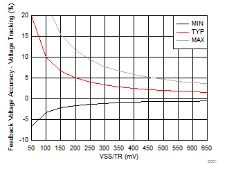
If a tracking function is desired, the SS/TR pin can be used for this purpose by connecting it to an external tracking voltage. The output voltage tracks that voltage with the typical gain and offset as specified in the electrical characteristics.
When the SS/TR pin voltage is above 0.7 V, the internal voltage is clamped and the device goes to normal regulation. This works for rising and falling tracking voltages with the same behavior, as long as the input voltage is inside the recommended operating conditions. For decreasing SS/TR pin voltage in PFM mode, the device does not sink current from the output. The resulting decrease of the output voltage may therefore be slower than the SS/TR pin voltage if the load is light. When driving the SS/TR pin with an external voltage, do not exceed the voltage rating of the SS/TR pin which is VIN + 0.3 V. The SS/TR pin is internally connected with a resistor to GND when EN = 0.
If the input voltage drops below undervoltage lockout, the output voltage will go to zero, independent of the tracking voltage. Figure 4 shows how to connect devices to get ratiometric and simultaneous sequencing by using the tracking function. See also Voltage Tracking in the systems examples. SS/TR is internally clamped to approximately 3 V.
The resistive divider of R5 and R6 can be used to change the ramp rate of VOUT2 to be faster, slower or the same as VOUT1.
A sequential startup is achieved by connecting the PG pin of VOUT of DEVICE 1 to the EN pin of DEVICE2. PG requires a pull-up resistor. Ratiometric start up sequence happens if both supplies are sharing the same Soft-Start capacitor. Equation 12 gives the Soft-Start time, though the SS/TR current has to be doubled. Details about these and other tracking and sequencing circuits are found in SLVA470.
Note: If the voltage at the FB pin is below its typical value of 0.7 V, the output voltage accuracy may have a wider tolerance than specified. The current of 2.5 µA out of the SS/TR pin also has an influence on the tracking function, especially for high resistive external voltage dividers on the SS/TR pin.
10.1.6 Output Filter and Loop Stability
The devices of the TPS6213X family are internally compensated to be stable with L-C filter combinations corresponding to a corner frequency to be calculated with Equation 13:

Proven nominal values for inductance and ceramic capacitance are given in Table 2 and are recommended for use. Different values may work, but care has to be taken on the loop stability which is affected. More information including a detailed LC stability matrix can be found in SLVA463.
The TPS62136x devices include an internal 15 pF feedforward capacitor, connected between the VOS and FB pins. This capacitor impacts the frequency behavior and sets a pole and zero in the control loop with the resistors of the feedback divider, per equation Equation 14 and Equation 15:


Though the TPS62136x devices are stable without the pole and zero being in a particular location, adjusting their location to the specific needs of the application can provide better performance in Power Save mode and/or improved transient response. An external feedforward capacitor can also be added. A more detailed discussion on the optimization for stability versus transient response can be found in SLVA289 and SLVA466.
10.2 Typical Applications
10.2.1 Typical Application with Adjustable Output Voltage
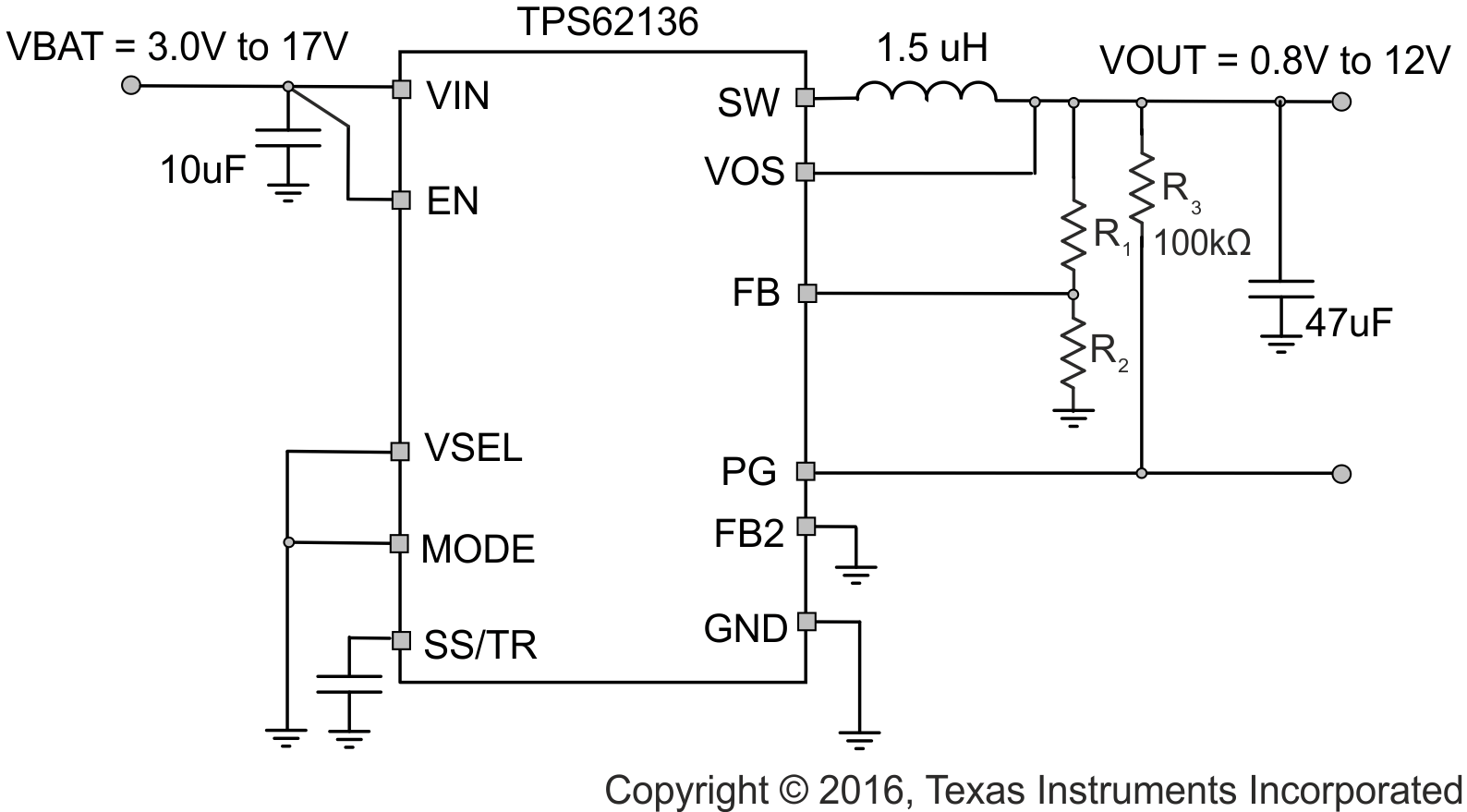 Figure 5. Typical Application
10.2.1.1 Design Requirements
The design guideline provides a component selection to operate the device within the recommended operating conditions. See Table 1 for the Bill of Materials used to generate the application curves.
10.2.1.2 Detailed Design Procedure

With VFB = 0.7 V:
Table 5. Setting the Output Voltage
| NOMINAL OUTPUT VOLTAGE | R1 | R2 | EXACT OUTPUT VOLTAGE |
|---|---|---|---|
| 0.8 V | 51 kΩ | 360 kΩ | 0.799 V |
| 1.2 V | 130 kΩ | 180 kΩ | 1.206 V |
| 1.5 V | 150 kΩ | 130 kΩ | 1.508 V |
| 1.8 V | 470 kΩ | 300 kΩ | 1.797 V |
| 2.5 V | 620 kΩ | 240 kΩ | 2.508 V |
| 3.3 V | 560 kΩ | 150 kΩ | 3.313 V |
| 5 V | 510 kΩ | 82 kΩ | 5.054 V |
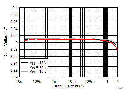
| 9 V | 510 kΩ | 43 kΩ | 9.002 V |
| 12 V | 1000 kΩ | 62 kΩ | 11.99 V |
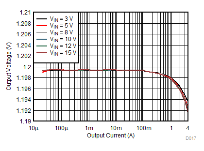
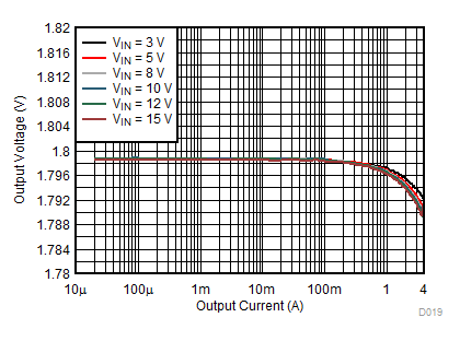
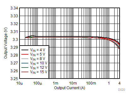
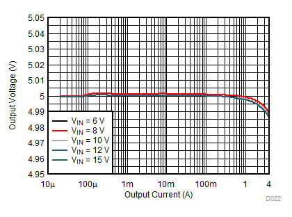
10.2.1.3 Application Curves
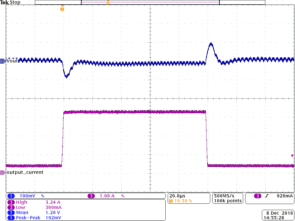
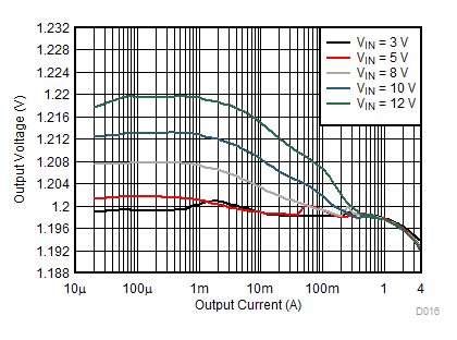
| Vin = 12 V; | PWM | Io = 350 mA to 3.1 A |
| Vout = 1.2 V | TA= 25 °C |
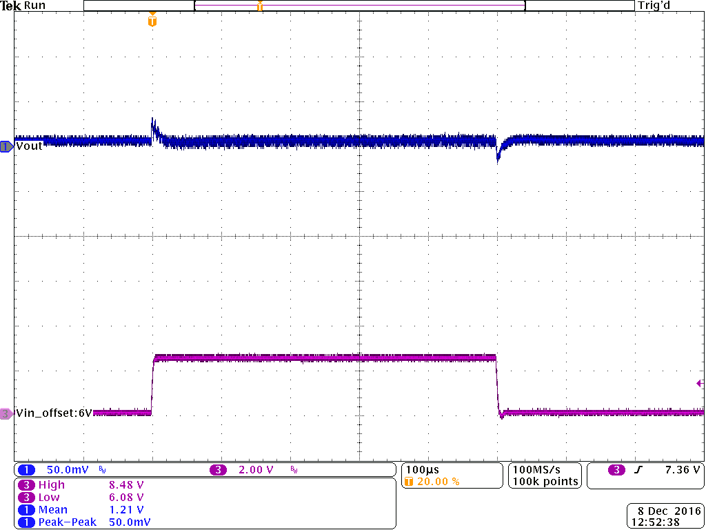
| Vin = 6 V to 8.4 V; | PWM | Io = 1 A |
| Vout = 1.2 V | TA= 25 °C |
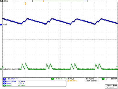
| Vin = 5 V; | PFM | Io = 0.1 A |
| Vout = 1.2 V | TA= 25 °C |
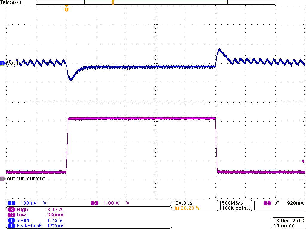
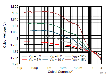
| Vout = 1.8 V | PFM | Io = 350 mA to 3.1 A |
| TA= 25 °C |
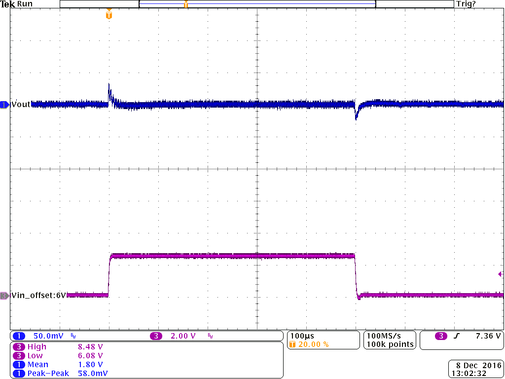
| Vin = 6 V to 8.4 V; | PFM | Io = 1 A |
| Vout = 1.8 V | TA= 25 °C |
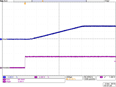
| Vout = 1.8 V | PFM | load current = 1A |
| TA= 25 °C |
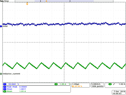
| Vout = 1.8 V | PWM | Io = 1 A |
| TA= 25 °C |
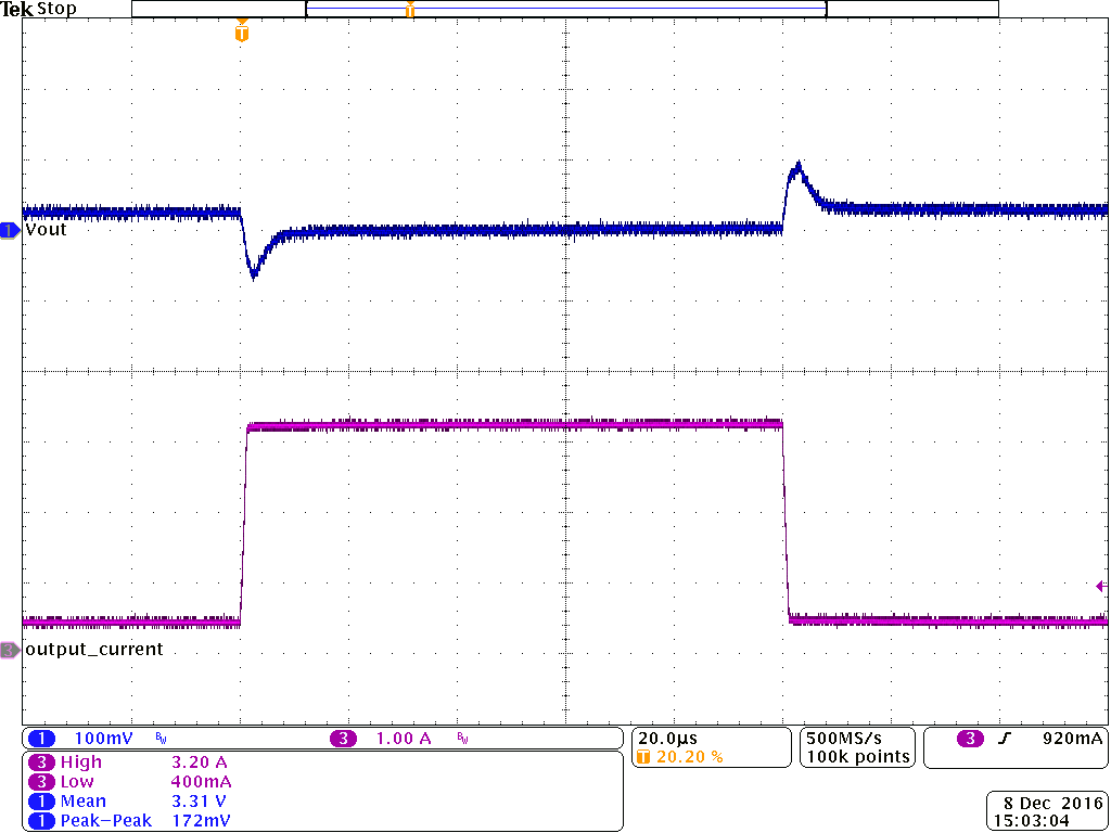
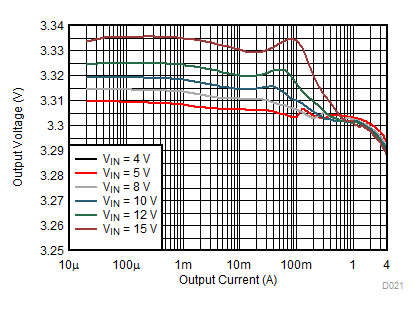
| Vout = 3.3 V | PWM | Io = 350 mA to 3.1 A |
| TA= 25 °C |
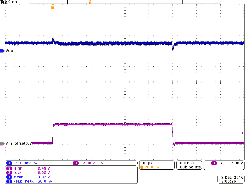
| Vin = 6 V to 8.4 V; | PWM | Io = 1 A |
| Vout = 3.3 V | TA= 25 °C |
.gif)
| Vout = 3.3 V | PFM | Io = 0.1 A |
| TA= 25 °C |
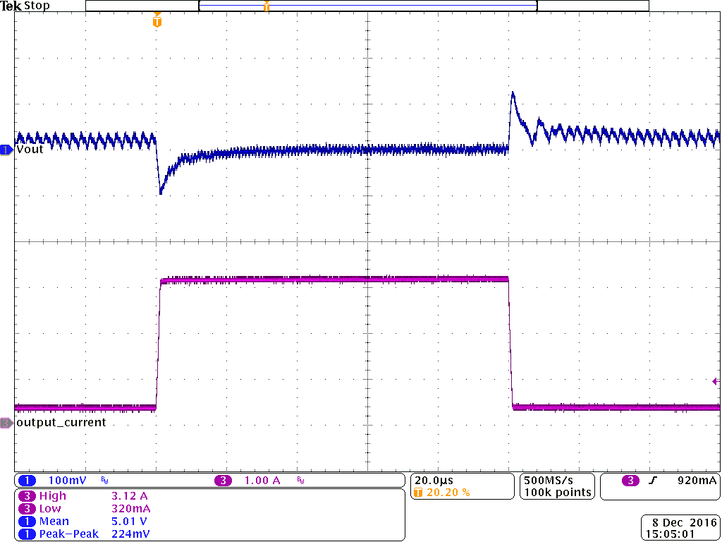
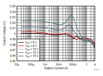
| Vout = 5 V | PFM | Io = 350 mA to 3.1 A |
| TA= 25 °C |
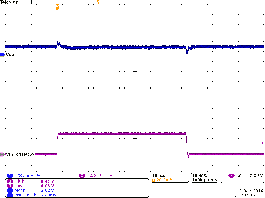
| Vin = 6 V to 8.4 V; | PFM | Io = 1 A |
| Vout = 5 V | TA= 25 °C |
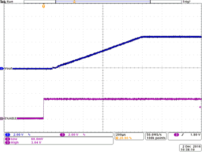
| Vout = 5 V | PFM | load current = 1A |
| TA= 25 °C |
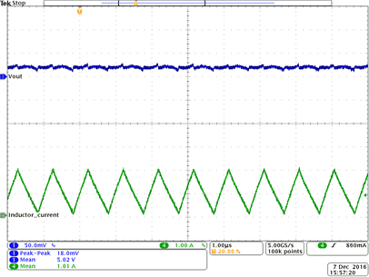
| Vout = 5 V | PWM | Io = 1 A |
| TA= 25 °C |
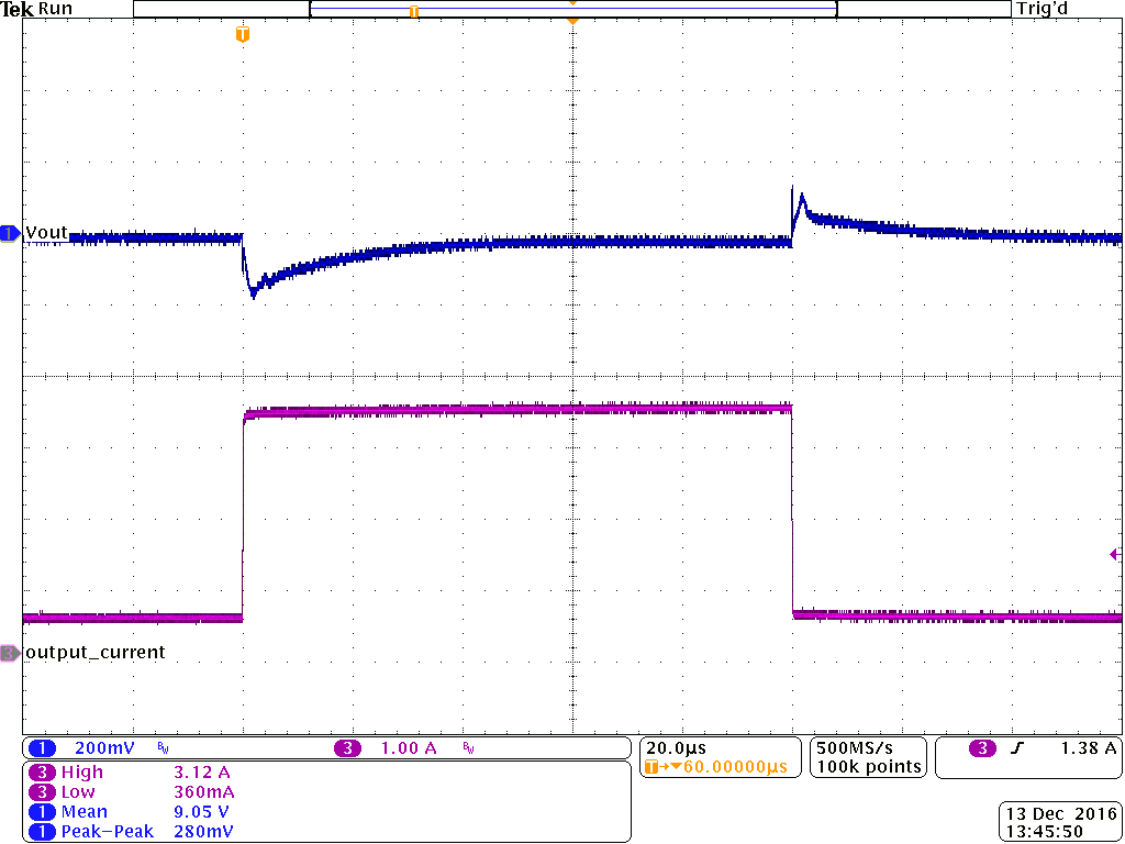
| Vout = 9 V | PWM | Io = 300 mA to 2.7 A |
| TA= 25 °C |
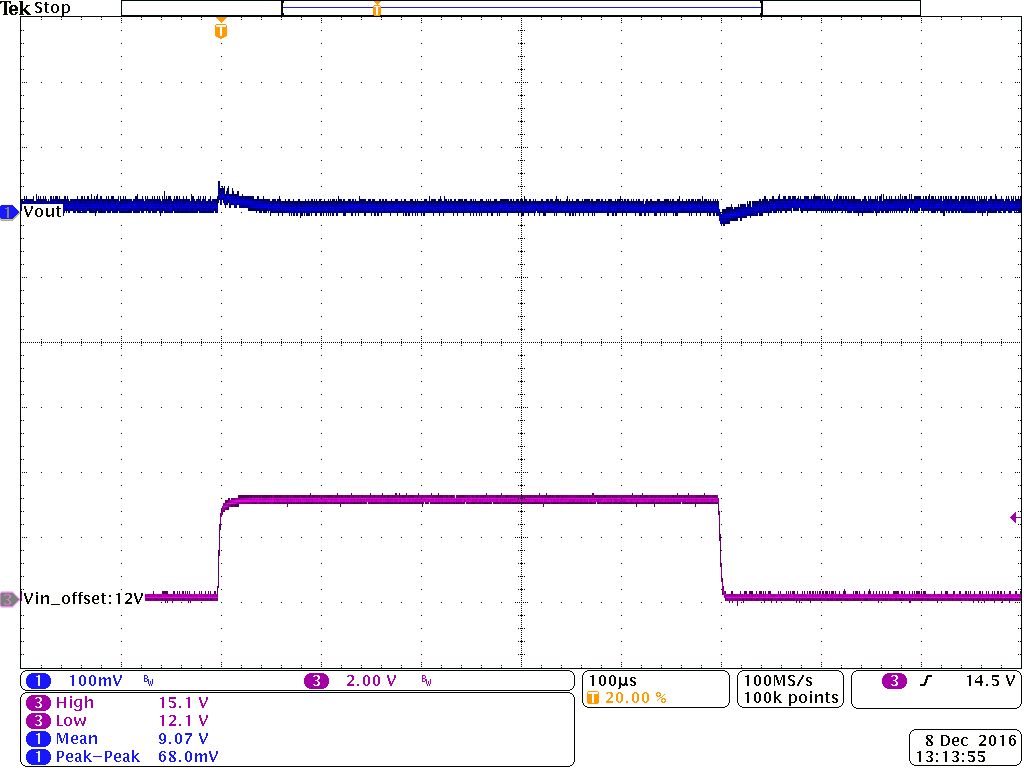
| Vin = 12 V to 15 V; | PWM | Io = 1 A |
| Vout = 9 V | TA= 25 °C |
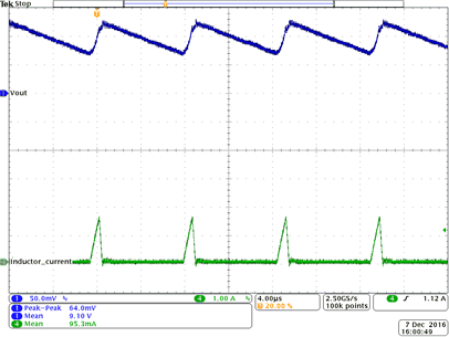
| Vout = 9 V | PFM | Io = 0.1 A |
| TA= 25 °C |
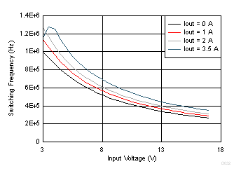
| Vout = 1.2 V | PWM | TA= 25 °C |
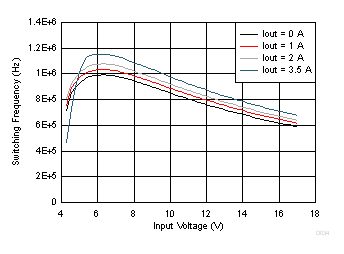
| Vout = 3.3 V | PWM | TA= 25 °C |
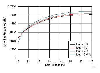
| Vout = 9 V | PWM | TA= 25 °C |
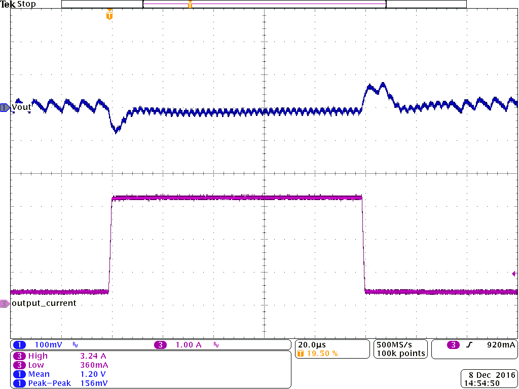
| Vin = 12 V; | PFM | Io = 350 mA to 3.1 A; |
| Vout = 1.2 V; | TA= 25 °C |
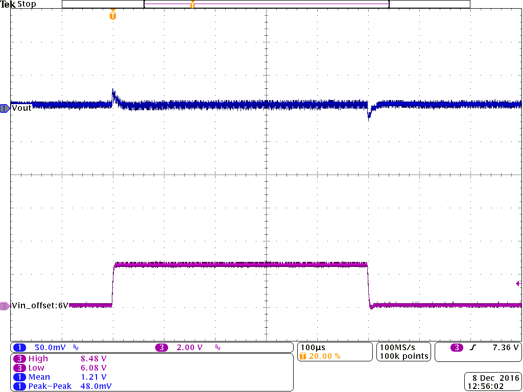
| Vin = 6 V to 8.4 V; | PFM | Io = 1 A |
| Vout = 1.2 V | TA= 25 °C |
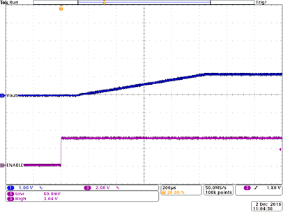
| Vin = 5 V; | PFM | load current = 1A |
| Vout = 1.2 V | TA= 25 °C |
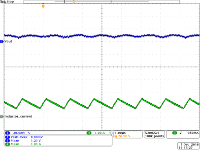
| Vin = 5 V; | PWM | Io = 1 A |
| Vout = 1.2 V | TA= 25 °C |
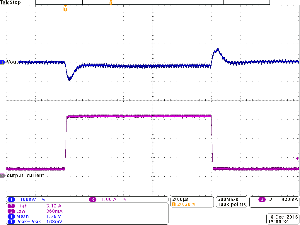
| Vout = 1.8 V | PWM | Io = 350 mA to 3.1 A |
| TA= 25°C |
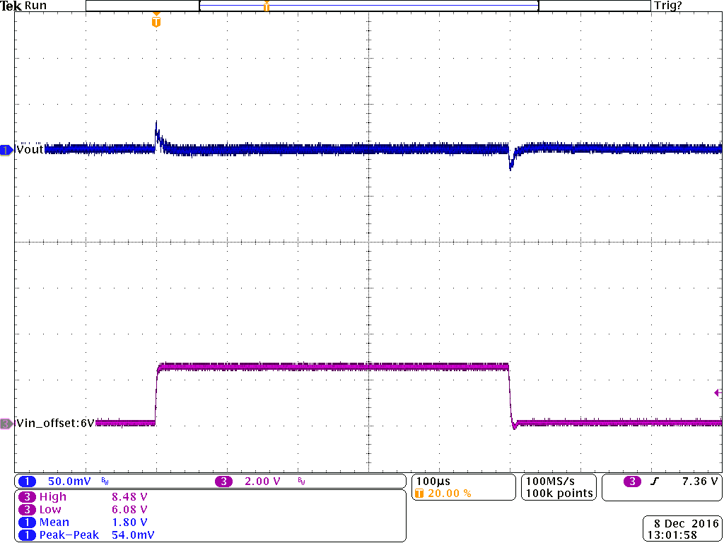
| Vin = 6 V to 8.4 V; | PWM | Io = 1 A |
| Vout = 1.8 V | TA= 25 °C |
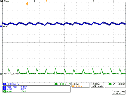
| Vout = 1.8 V | PFM | Io = 0.1 A |
| TA= 25 °C |
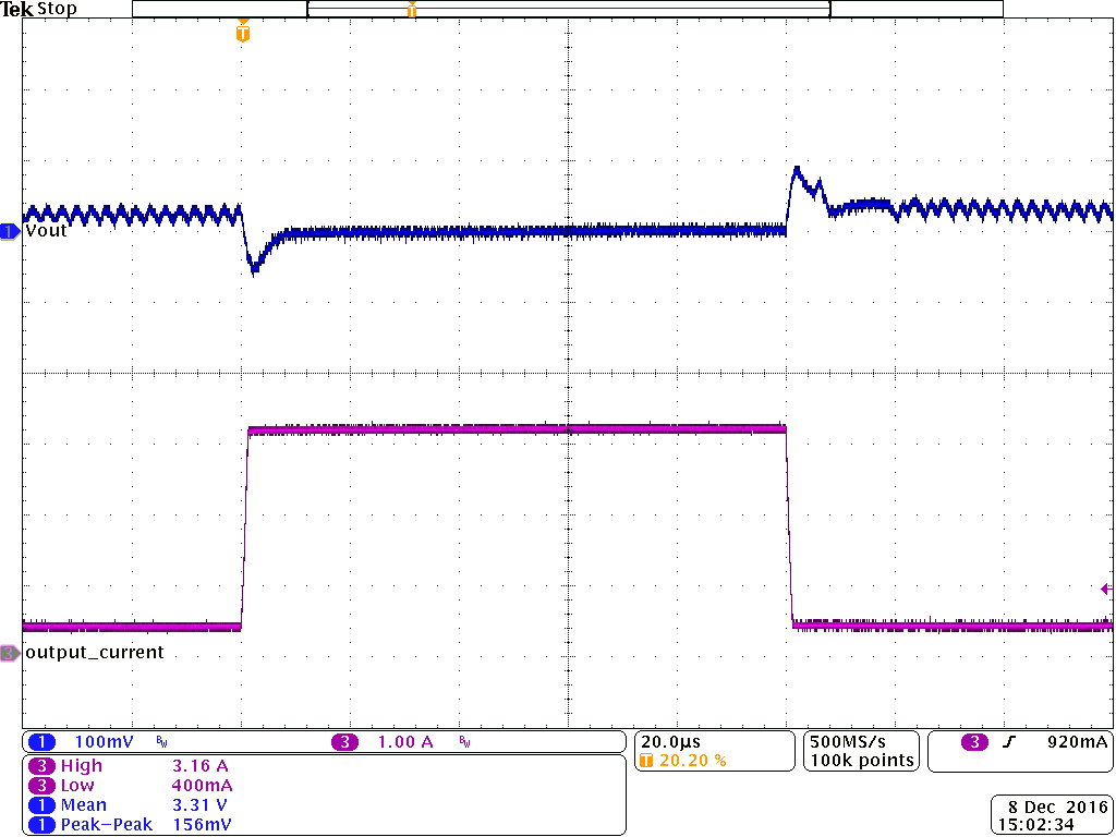
| Vout = 3.3 V | PFM | Io = 350 mA to 3.1 A |
| TA= 25 °C |
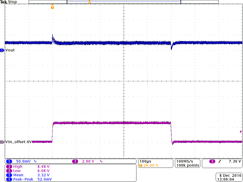
| Vin = 6 V to 8.4 V; | PFM | Io = 1 A |
| Vout = 3.3 V | TA= 25 °C |
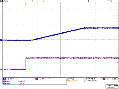
| Vout = 3.3 V | PFM | load current = 1A |
| TA= 25 °C |
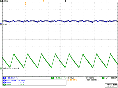
| Vout = 3.3 V | PWM | Io = 1 A |
| TA= 25 °C |
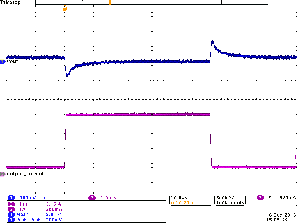
| Vout = 5 V | PWM | Io = 350 mA to 3.1 A |
| TA= 25 °C |
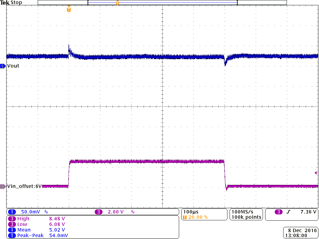
| Vin = 6 V to 8.4 V; | PWM | Io = 1 A |
| Vout = 5 V | TA= 25 °C |
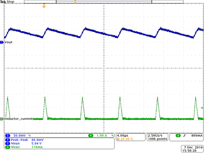
| Vout = 5 V | PFM | Io = 0.1 A |
| TA= 25 °C |
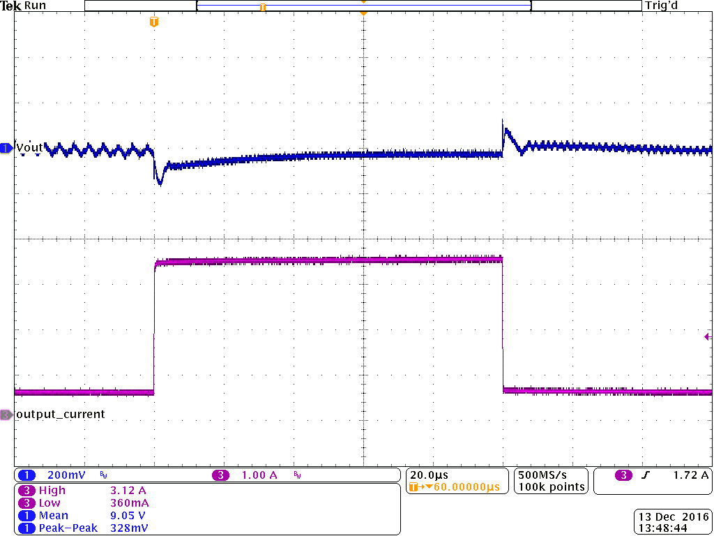
| Vout = 9 V | PFM | Io = 300 mA to 2.7 A |
| TA= 25 °C |
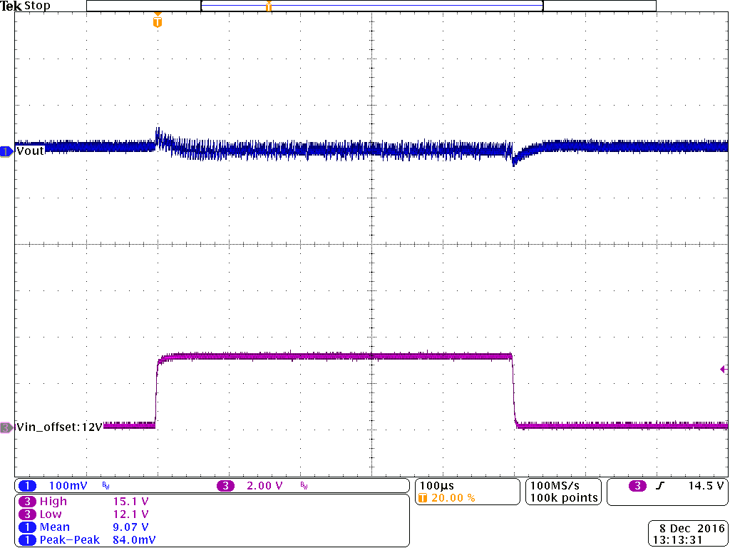
| Vin = 12 V to 15 V; | PFM | Io = 1 A |
| Vout = 9 V | TA= 25 °C |
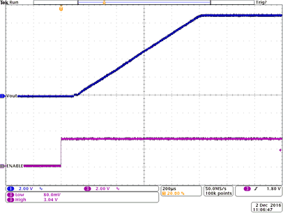
| Vout = 9 V | PFM | load current = 1A |
| TA= 25 °C |
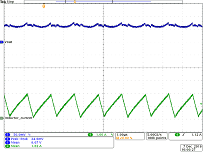
| Vout = 9 V | PWM | Io = 1 A |
| TA= 25 °C |
10.2.2 Typical Application using VSEL and FB2
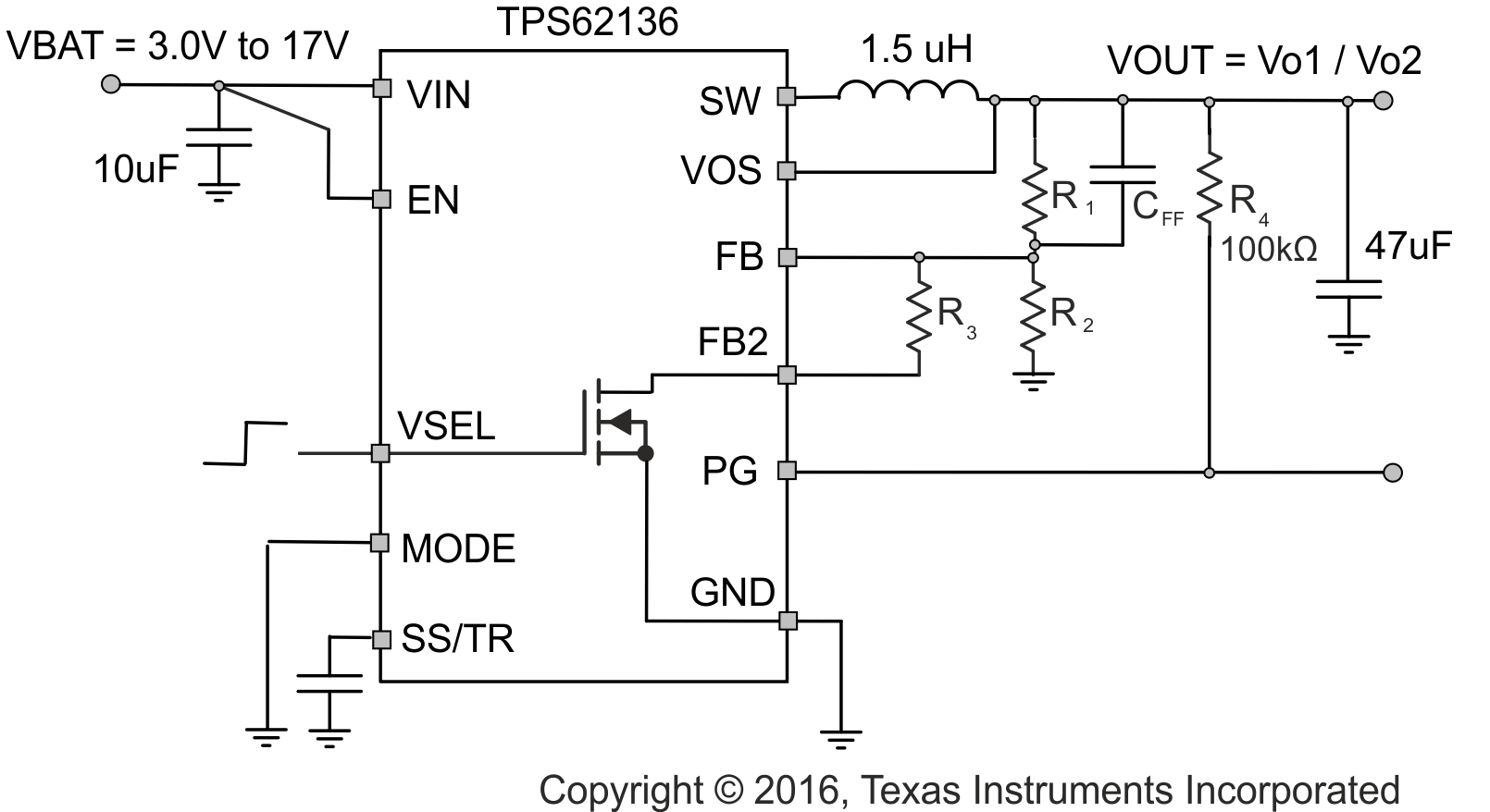 Figure 72. Typical Application using VSEL
10.2.2.1 Design Requirements
VSEL allows to switch between two output voltages by changing the output voltage divider ratio. This is done by an internal MOSFET connecting resistor R3 to GND. Pulling VSEL high turns on the MOSFET that connects R3 in parallel to R2. The divider ratio is changed such that the output voltage increases from Vo1 to Vo2.
When the output voltage is ramped down and the device is in forced PWM mode, the device will sink current.
10.2.2.2 Detailed Design Procedure
TPS62136x typically does not require a feed forward capacitor in parallel to R1. For a large voltage change such as 3.3 V to 5 V, a small feed forward capacitor CFFhelps to improve the settling behavior. In order to switch from an output voltage of for example 3.3 V to an output voltage of 5 V, set the resistor divider for R1 and R2 to 3.3V and calculate R3 with Equation 17. With R1 = 560 kΩ and R2 = 150 kΩ this gives R3 = 232 kΩ. A feedforward capacitor of 12 pF was used to get a voltage transition as shown below.

10.2.2.3 Application Curves
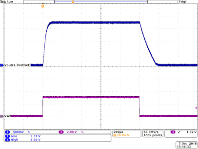 Figure 73. Output Voltage Change from 3.3 V to 5 V in PFM with 20 Ω load resistance
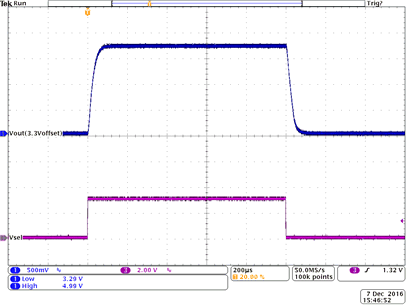 Figure 74. Output Voltage Change from 3.3 V to 5 V in PWM with 20 Ω load resistance
10.3 System Examples
10.3.1 LED Power Supply
The TPS62136x can be used as a power supply for power LEDs. The FB pin can be easily set down to lower values than nominal by using the SS/TR pin. With that, the voltage drop on the sense resistor is low to avoid excessive power loss. Since this pin provides 2.5 µA, the feedback pin voltage can be adjusted by an external resistor per Equation 18. This drop, proportional to the LED current, is used to regulate the output voltage (anode voltage) to a proper level to drive the LED. Both analog and PWM dimming are supported with the TPS62136x. Figure 75 shows an application circuit, tested with analog dimming:
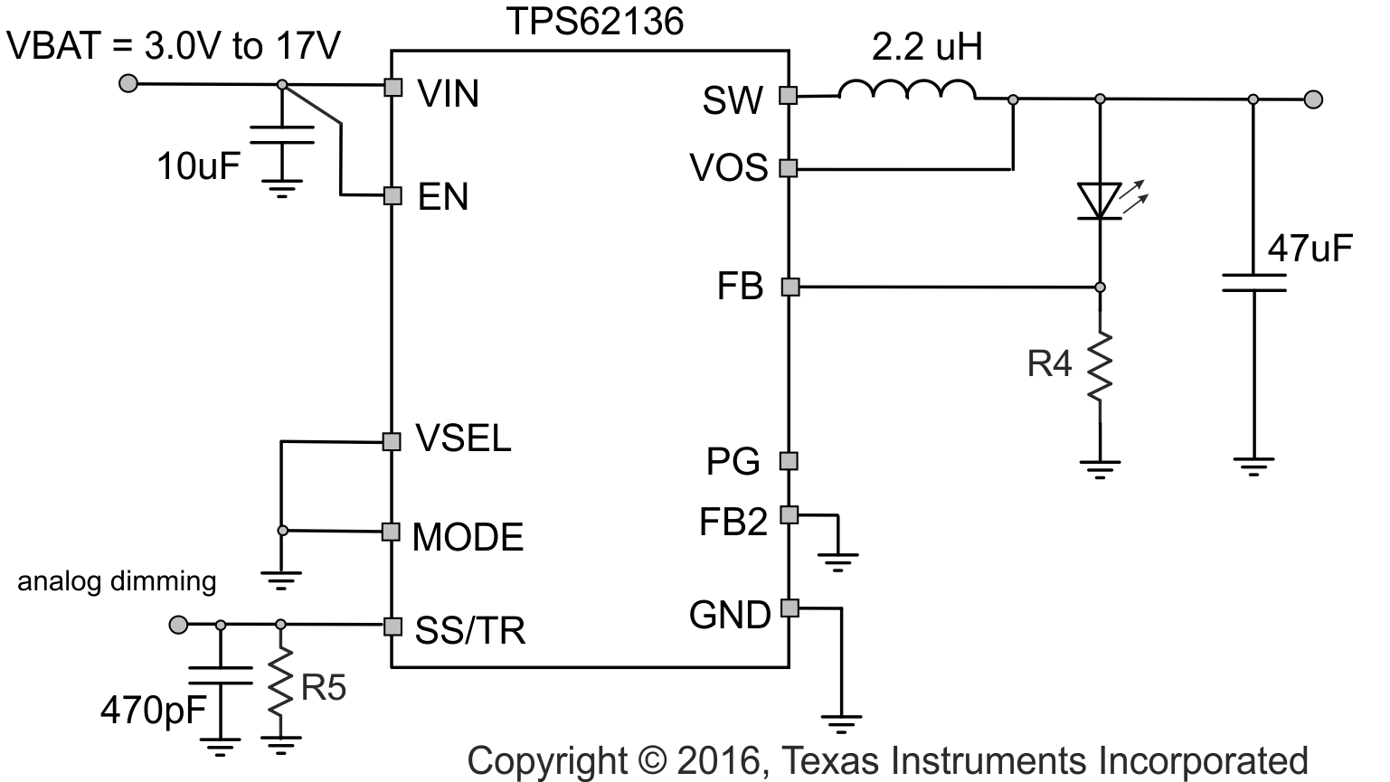 Figure 75. Single Power LED Supply
spacing
The resistor at SS/TR defines the FB voltage. It is set to 350 mV by R5 = 140 kΩ using Equation 18. This cuts the losses on R4 to half from the nominal 0.7 V of feedback voltage while it still provides good accuracy.
spacing

spacing
The device now supplies a constant current set by resistor R4 from FB to GND. The minimum input voltage has to be rated according the forward voltage needed by the LED used. More information is available in the Application Note SLVA451.
spacing
10.3.2 Powering Multiple Loads
In applications where TPS62136x is used to power multiple load circuits, it may be the case that the total capacitance on the output is very large. In order to properly regulate the output voltage, there needs to be an appropriate AC signal level on the VOS pin. Tantalum capacitors have a large enough ESR to keep output voltage ripple sufficiently high on the VOS pin. With low ESR ceramic capacitors, the output voltage ripple may get very low, so it is not recommended to use a large capacitance directly on the output of the device. If there are several load circuits with their associated input capacitor on a pcb, these loads are typically distributed across the board. This adds enough trace resistance (Rtrace) to keep a large enough AC signal on the VOS pin for proper regulation.
The minimum total trace resistance on the distributed load is 10 mΩ. The total capacitance n x Cin in the use case below was 32 x 47 uF of ceramic X7R capacitors.
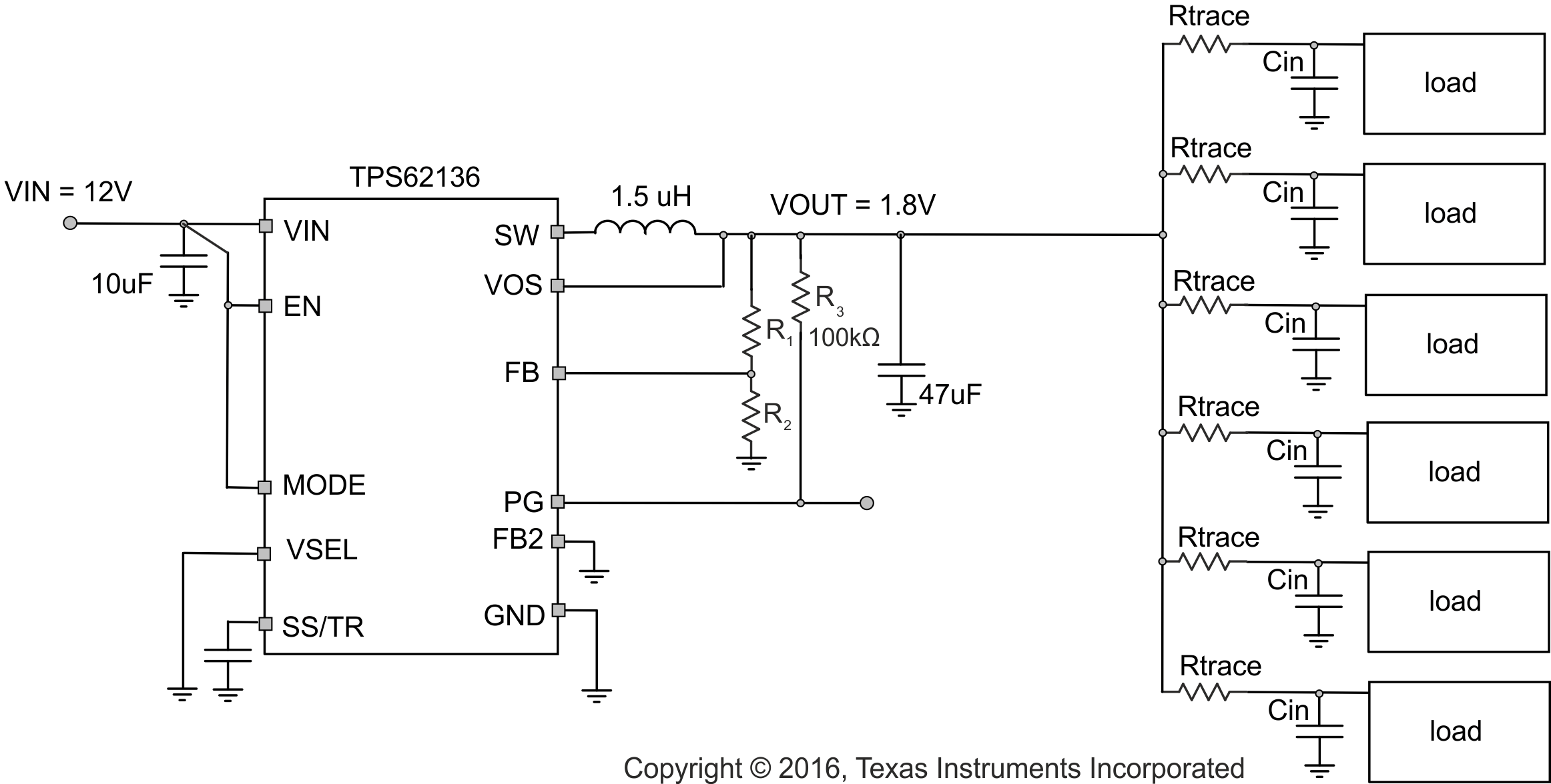 Figure 76. Multiple Loads
10.3.3 Voltage Tracking
DEVICE 2 follows the voltage applied to the SS/TR pin. A ramp on SS/TR to 0.7 V ramps the output voltage according to the 0.7 V reference.
Tracking the 3.3 V of DEVICE 1 requires a resistor divider on SS/TR of DEVICE 2 equal to the output voltage divider of DEVICE 1. The output current of 2.5µA from the SS/TR pin cases an offset voltage on the resistor divider formed by R5 and R6. The equivalent resistance of R6 // R5 should therefore be kept below 15kΩ.
10.3.4 Precise Soft-Start Timing
The SS/TR pin of the TPS62136x can be used for tracking as well as for setting the Soft-Start time. The TPS62136x has one GND terminal which is used for the power ground as well as for the analog ground connection. While starting the device with a load current above approximately 1 A, the noise on the GND connection can lead to a Soft-Start time shorter than calculated. There are two external work arounds as given below.
Adding a 10 kΩ resistor filters the noise on the GND connection and keeps the Soft-Start time at the value calculated.
Figure 80 does not require an external component. It provides a connection to the internal analog ground by using the FB2 pin and its internal NMOS to that node. The internal NMOS needs to be turned ON by setting VSEL = high.
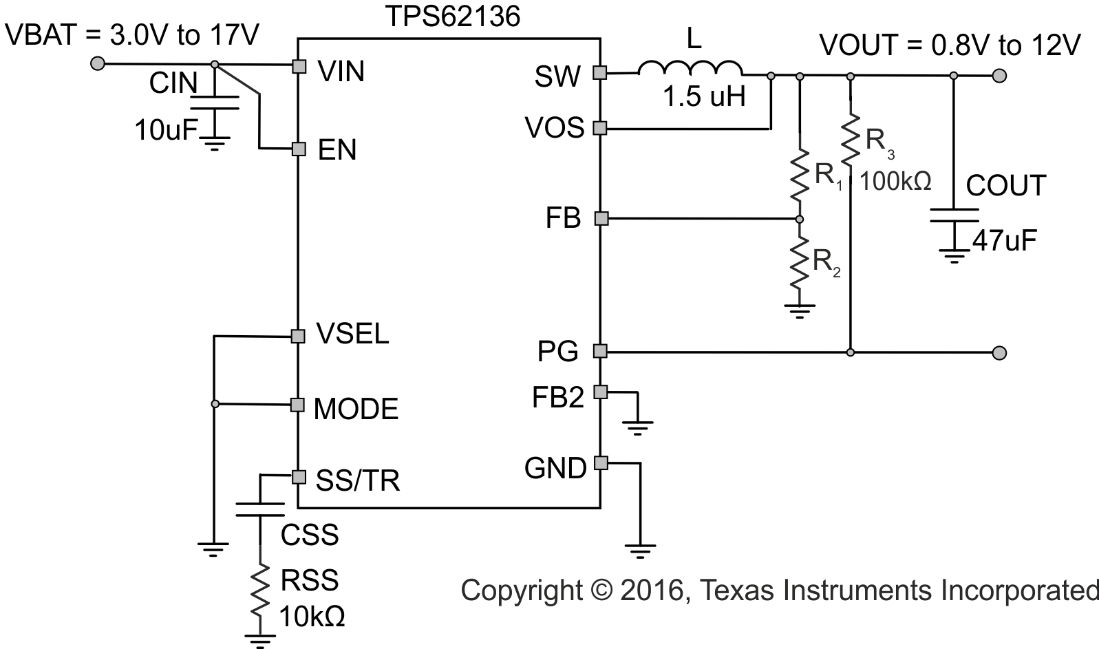 Figure 79. Adding a Series Resistor to CSS
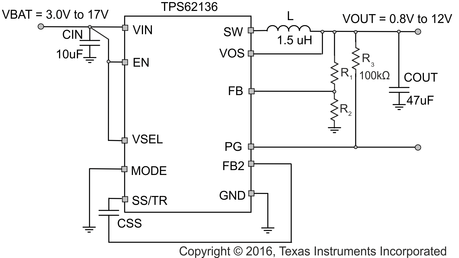 Figure 80. Connecting CSS to the Internal Analog Ground by using FB2
