ZHCSMB6E March 2010 – October 2020 TPS62065 , TPS62067
PRODUCTION DATA
- 1 特性
- 2 应用
- 3 说明
- 4 Revision History
- 5 Device Comparison Table
- 6 Pin Configuration and Functions
- 7 Specifications
- 8 Detailed Description
- 9 Application and Implementation
- 10Power Supply Recommendations
- 11Layout
- 12Device and Documentation Support
- 13Mechanical, Packaging, and Orderable Information
9.2.3 Application Curves
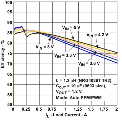 Figure 9-2 VOUT = 1.2 V, Auto PFM/PWM Mode, Linear Scale
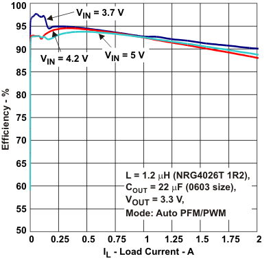 Figure 9-4 VOUT = 3.3 V, Auto PFM/PWM Mode, Linear Scale
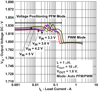 Figure 9-6 Auto PFM/PWM Mode
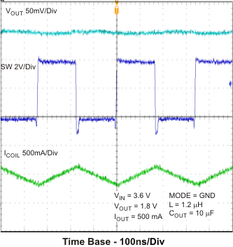 Figure 9-8 Typical Operation (PWM Mode)
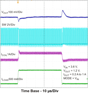 Figure 9-10 Load Transient Response PWM Mode 0.2 A to 1 A
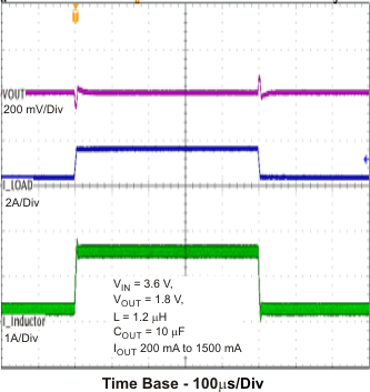 Figure 9-12 Load Transient Response 200 mA to 1500 mA
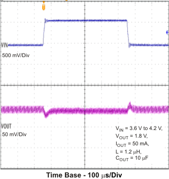 Figure 9-14 Line Transient PFM Mode
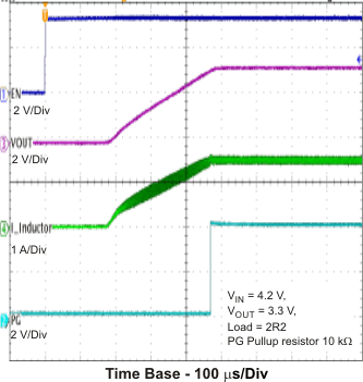 Figure 9-16 Start-up TPS62067 Into 2.2-Ω Load With Power Good
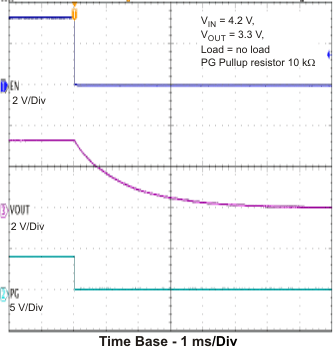 Figure 9-18 Shutdown TPS62067
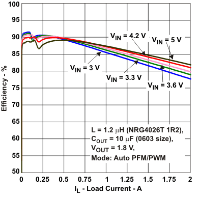 Figure 9-3 VOUT = 1.8 V, Auto PFM/PWM Mode, Linear Scale
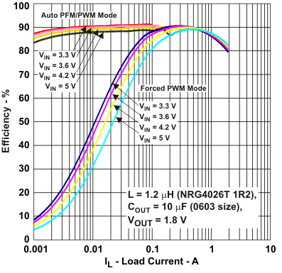 Figure 9-5 Auto PFM/PWM Mode vs. Forced PWM Mode, Logarithmic Scale
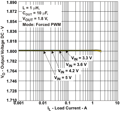 Figure 9-7 Forced PWM Mode
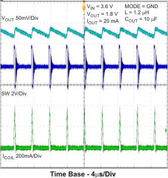 Figure 9-9 Typical Operation (PFM Mode)
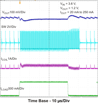 Figure 9-11 Load Transient PFM Mode 20 mA to 250 mA
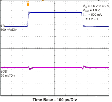 Figure 9-13 Line Transient Response PWM Mode
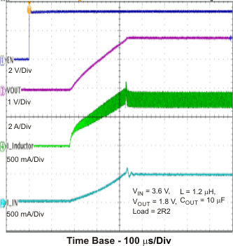 Figure 9-15 Startup Into Load – VOUT 1.8 V
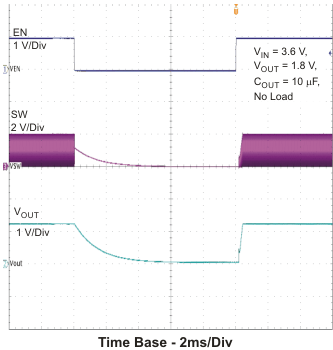 Figure 9-17 Output Discharge