ZHCSD80B january 2015 – august 2023 TPS62065-Q1 , TPS62067-Q1
PRODUCTION DATA
- 1
- 1 特性
- 2 应用
- 3 说明
- 4 Revision History
- 5 Device Comparison Table
- 6 Pin Configuration and Functions
- 7 Specifications
- 8 Parameter Measurement Information
-
9 Detailed Description
- 9.1 Overview
- 9.2 Functional Block Diagram
- 9.3
Feature Description
- 9.3.1 Mode Selection (TPS62065-Q1) and Forced PWM Mode (TPS62067A-Q1)
- 9.3.2 Power Good (PG, TPS62067x-Q1)
- 9.3.3 Enable
- 9.3.4 Shutdown and Output Discharge
- 9.3.5 Soft Start
- 9.3.6 Undervoltage Lockout (UVLO)
- 9.3.7 Internal Current Limit and Foldback Current Limit For Short-Circuit Protection
- 9.3.8 Clock Dithering
- 9.3.9 Thermal Shutdown
- 9.4 Device Functional Modes
- 10Application and Implementation
- 11Device and Documentation Support
- 12Mechanical, Packaging, and Orderable Information
6 Pin Configuration and Functions
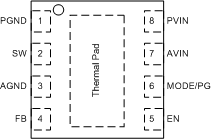
 Figure 6-1 DSG Package8-Pin WSON With Exposed Thermal PadTop View
Table 6-1 Pin Functions
| PIN | TYPE | DESCRIPTION | |
|---|---|---|---|
| NO. | NAME | ||
| 1 | PGND | — | GND supply pin for the output stage |
| 2 | SW | OUT | This pin is the switch pin and is connected to the internal MOSFET switches. Connect the external inductor between this terminal and the output capacitor. |
| 3 | AGND | — | Analog GND supply pin for the control circuit |
| 4 | FB | IN | Feedback pin for the internal regulation loop. Connect the external resistor divider to this pin. In case of the fixed output voltage option, connect this pin directly to the output capacitor. |
| 5 | EN | IN | This pin is the enable pin of the device. Pulling this pin to low forces the device into shutdown mode. Pulling this pin to high enables the device. This pin must be terminated. |
| 6 | MODE/PG | IN | MODE: MODE pin = high forces the device to operate in fixed frequency PWM mode. MODE pin = low enables the power save mode with automatic transition from PFM mode to fixed frequency PWM mode. This pin must be terminated. (TPS62065-Q1) |
| Open Drain | PG: Power Good open-drain output. Connect an external pullup resistor to a rail which is below or equal AVIN. (TPS62067-Q1) | ||
| 7 | AVIN | IN | Analog VIN power supply for the control circuit must be connected to PVIN and input capacitor. |
| 8 | PVIN | PWR | VIN power supply pin for the output stage |
| — | Thermal Pad | — | For good thermal performance, this pad must be soldered to the land pattern on the PCB. Use this pad as device GND. |