ZHCSID4B June 2018 – January 2021 TPS61372
PRODUCTION DATA
- 1 特性
- 2 应用
- 3 说明
- 4 Revision History
- 5 Pin Configuration and Functions
- 6 Specifications
- 7 Detailed Description
-
8 Application and Implementation
- 8.1 Application Information
- 8.2
Typical Application
- 8.2.1 Design Requirements
- 8.2.2
Detailed Design Procedure
- 8.2.2.1 Custom Design With WEBENCH® Tools
- 8.2.2.2 Setting the Output Voltage
- 8.2.2.3 Selecting the Inductor
- 8.2.2.4 Selecting the Output Capacitors
- 8.2.2.5 Selecting the Input Capacitors
- 8.2.2.6 Loop Stability and Compensation
- 8.2.2.7 Loop Compensation Design Steps
- 8.2.2.8 Selecting the Bootstrap Capacitor
- 8.2.3 Application Curves
- 9 Power Supply Recommendations
- 10Layout
- 11Device and Documentation Support
- 12Mechanical, Packaging, and Orderable Information
8.2.2.6.1 Small Signal Model
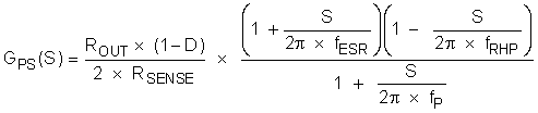
The TPS61372 uses the peak current with adaptive off-time control topology. With the inductor current information sensed, the small-signal model of the power stage reduces from a two-pole system, created by L and COUT, to a single-pole system, created by ROUT and COUT. An external loop compensation network connecting to the COMP pin of TPS61372 is added to optimize the loop stability and the response time, a resistor RC, capacitor CC, and CP shown in Figure 8-2 comprises the loop compensation network.
 Figure 8-2 TPS61372 Control Equivalent Circuitry Model
The small signal of power stage including the slope compensation is:
where
- D is the duty cycle
- ROUT is the output load resistor
- RSENSE is the equivalent internal current sense resistor, which is typically 0.2 Ω of TPS61372
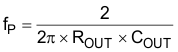
The single pole of the power stage is:
where
- COUT is the output capacitance, for a boost converter having multiple, identical output capacitors in parallel, simply combine the capacitors with the equivalent capacitance
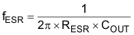
The zero created by the ESR of the output capacitor is:
where
- RESR is the equivalent resistance in series of the output capacitor
The right-hand plane zero is:
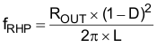
where
- D is the duty cycle
- ROUT is the output load resistor
- L is the inductance
The TPS61372 COMP pin is the output of the internal trans-conductance amplifier.
Equation 15 shows the equation for feedback resistor network and the error amplifier.
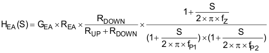
where
- REA is the output impedance of the error amplifier REA = 500 MΩ. GEA is the transconuctance of the error amplifier, GEA = 175 μS.
- ƒP1, ƒP2 is the pole's frequency of the compensation
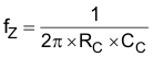
- fZ is the zero’s frequency of the compensation network
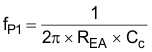
where
- CC is the zero capacitor compensation
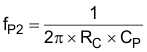
where
- CP is the pole capacitor compensation
- RC is the resistor of the compensation network