ZHCSHT5A July   2011  – March 2018 TPS61256A

PRODUCTION DATA.  

  1. 特性
  2. 应用范围
  3. 说明
    1.     Device Images
      1.      最小解决方案尺寸应用
      2.      效率与负载电流间的关系
  4. 修订历史记录
  5. Pin Configuration and Functions
    1.     Pin Functions
  6. Specifications
    1. 6.1 Absolute Maximum Ratings
    2. 6.2 ESD Ratings
    3. 6.3 Recommended Operating Conditions
    4. 6.4 Thermal Information
    5. 6.5 Electrical Characteristics
    6. 6.6 Typical Characteristics
  7. Parameter Measurement Information
  8. Detailed Description
    1. 8.1 Overview
    2. 8.2 Softstart
    3. 8.3 Undervoltage Lockout
    4. 8.4 Thermal Regulation
    5. 8.5 Thermal Shutdown
    6. 8.6 Functional Block Diagram
    7. 8.7 Feature Description
      1. 8.7.1 Power-Save Mode
      2. 8.7.2 Current Limit Operation
      3. 8.7.3 Enable
      4. 8.7.4 Load Disconnect And Reverse Current Protection
    8. 8.8 Device Functional Modes
      1. 8.8.1 Load Disconnect And Reverse Current Protection
      2. 8.8.2 Softstart
      3. 8.8.3 Undervoltage Lockout
      4. 8.8.4 Thermal Regulation
      5. 8.8.5 Thermal Shutdown
  9. Application and Implementation
    1. 9.1 Application Information
    2. 9.2 Typical Application
      1. 9.2.1 Design Requirements
      2. 9.2.2 Detailed Design Procedure
        1. 9.2.2.1 Inductor Selection
          1. 9.2.2.1.1 High-frequency Converter Applications
        2. 9.2.2.2 Output Capacitor
        3. 9.2.2.3 Input Capacitor
        4. 9.2.2.4 Checking Loop Stability
      3. 9.2.3 Application Curves
  10. 10Power Supply Recommendations
  11. 11Layout
    1. 11.1 Layout Guidelines
    2. 11.2 Layout Example
    3. 11.3 Thermal Information
  12. 12Package Summary
    1. 12.1 Package Dimensions
  13. 13器件和文档支持
    1. 13.1 器件支持
      1. 13.1.1 第三方产品免责声明
    2. 13.2 接收文档更新通知
    3. 13.3 社区资源
    4. 13.4 商标
    5. 13.5 静电放电警告
    6. 13.6 Glossary
  14. 14机械、封装和可订购信息

封装选项

请参考 PDF 数据表获取器件具体的封装图。

机械数据 (封装 | 引脚)
  • YFF|9
散热焊盘机械数据 (封装 | 引脚)
订购信息

Current Limit Operation

The TPS61256A device employs a valley current limit sensing scheme. Current limit detection occurs during the off-time by sensing of the voltage drop across the synchronous rectifier.

The output voltage is reduced as the power stage of the device operates in a constant current mode. The maximum continuous output current (IOUT(CL)), before entering current limit (CL) operation, can be defined by Equation 1.

Equation 1. TPS61256A eq1_IOUT_DD_lvsag8.gif

The duty cycle (D) can be estimated by Equation 2

Equation 2. TPS61256A eq2_D_DD_lvs956.gif

and the peak-to-peak current ripple (ΔIL) is calculated by Equation 3

Equation 3. TPS61256A eq3_diL_DD_lvs956.gif

The output current, IOUT(DC), is the average of the rectifier ripple current waveform. When the load current is increased such that the lower peak is above the current limit threshold, the off-time is increased to allow the current to decrease to this threshold before the next on-time begins (so called frequency fold-back mechanism). When the current limit is reached the output voltage decreases during further load increase.

illustrates the inductor and rectifier current waveforms during current limit operation.
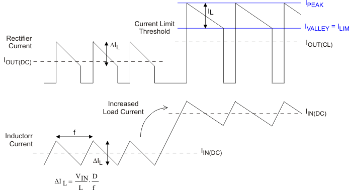
TPS61256A ind_cur_lvsag8.gifFigure 13. Inductor/Rectifier Currents In Current Limit Operation