SLVS937C March 2009 – July 2016 TPS61160A , TPS61161A
PRODUCTION DATA.
- 1 Features
- 2 Applications
- 3 Description
- 4 Revision History
- 5 Pin Configuration and Functions
- 6 Specifications
- 7 Detailed Description
- 8 Application and Implementation
- 9 Power Supply Recommendations
- 10Layout
- 11Device and Documentation Support
- 12Mechanical, Packaging, and Orderable Information
7 Detailed Description
7.1 Overview
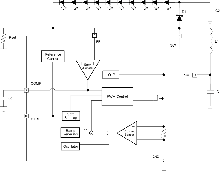
The TPS61160A/61A is a high-efficiency, high output voltage boost converter in small package size that is ideal for driving white LED in series. The serial LED connection provides even illumination by sourcing the same output current through all LEDs, eliminating the need for expensive factory calibration. The device integrates 40-V/0.7-A switch FET and operates in pulse width modulation (PWM) with 600-kHz fixed switching frequency. For operation see the block diagram. The duty cycle of the converter is set by the error amplifier output and the current signal applied to the PWM control comparator. The control architecture is based on traditional current-mode control; therefore, a slope compensation is added to the current signal to allow stable operation for duty cycles larger than 50%. The feedback loop regulates the FB pin to a low reference voltage (200 mV typical), reducing the power dissipation in the current sense resistor.
7.2 Functional Block Diagram

7.3 Feature Description
7.3.1 Soft Start-Up
Soft-start circuitry is integrated into the IC to avoid a high inrush current during start-up. After the device is enabled, the voltage at FB pin ramps up to the reference voltage in 32 steps, each step takes 213 μs. This ensures that the output voltage rises slowly to reduce the input current. Additionally, for the first 5 msec after the COMP voltage ramps, the current limit of the switch is set to half of the normal current limit spec. During this period, the input current is kept below 400 mA (typical). See the start-up waveform of a typical example, Figure 9.
7.3.2 Open LED Protection
Open LED protection circuitry prevents IC damage as the result of white LED disconnection. The TPS61160A/61A monitors the voltage at the SW pin and FB pin during each switching cycle. The circuitry turns off the switch FET and shuts down the IC when both of the following conditions persist for 8 switching clock cycles: (1) the SW voltage exceeds the VOVP threshold and (2) the FB voltage is less than half of regulation voltage. As a result, the output voltage falls to the level of the input supply. The device remains in shutdown mode until it is enabled by toggling the CTRL pin logic. To allow the use of inexpensive low-voltage output capacitor, the TPS61160A/61A has different open lamp protection thresholds. The threshold is set at 26 V for the TPS61160A and 38 V for the TPS61161A. Select the appropriate device so that the product of the number of external LEDs and each LED's maximum forward voltage plus the 200 mV reference voltage does not exceed the minimum OVP threshold or (nLEDS X VLED(MAX)) + 200 mV ≤ VOVP(MIN).
7.3.3 Shutdown
The TPS61160A/61A enters shutdown mode when the CTRL voltage is logic low for more than 2.5 ms. During shutdown, the input supply current for the device is less than 1 μA (max). Although the internal FET does not switch in shutdown, there is still a DC current path between the input and the LEDs through the inductor and Schottky diode. The minimum forward voltage of the LED array must exceed the maximum input voltage to ensure that the LEDs remain off in shutdown; however, in the typical application with two or more LEDs, the forward voltage is large enough to reverse bias the Schottky and keep leakage current low.
7.3.4 Current Program
The FB voltage is regulated by a low 0.2-V reference voltage. The LED current is programmed externally using a current-sense resistor in series with the LED string. The value of the RSET is calculated using Equation 1:

where
- ILED = output current of LEDs
- VFB = regulated voltage of FB
- RSET = current sense resistor
The output current tolerance depends on the FB accuracy and the current sensor resistor accuracy.
7.3.5 PWM Brightness Dimming
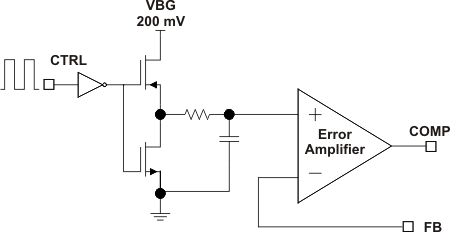
When the CTRL pin is constantly high, the FB voltage is regulated to 200 mV typically. However, the CTRL pin allows a PWM signal to reduce this regulation voltage; therefore, it achieves LED brightness dimming. The relationship between the duty cycle and FB voltage is given by Equation 2.

where
- Duty = duty cycle of the PWM signal
- 200 mV = internal reference voltage
As shown in Figure 11, the IC chops up the internal 200-mV reference voltage at the duty cycle of the PWM signal. The pulse signal is then filtered by an internal low pass filter. The output of the filter is connected to the error amplifier as the reference voltage for the FB pin regulation. Therefore, although a PWM signal is used for brightness dimming, only the WLED DC current is modulated, which is often referred as analog dimming. This eliminates the audible noise which often occurs when the LED current is pulsed in replica of the frequency and duty cycle of PWM control. Unlike other scheme which filters the PWM signal for analog dimming, TPS61160A/61A regulation voltage is independent of the PWM logic voltage level which often has large variations.
For optimum performance, use the PWM dimming frequency in the range of 5 kHz to 100 kHz. The requirement of minimum dimming frequency comes from the output ripple. Low frequency causes high output ripple. Because the CTRL pin is logic only pin, applying an external RC filter to the pin does not work.
To use lower PWM dimming, add an external RC network connected to the FB pin as shown in Figure 15).
7.3.6 Undervoltage Lockout
An undervoltage lockout prevents operation of the device at input voltages below typical 2.2 V. When the input voltage is below the undervoltage threshold, the device is shutdown and the internal switch FET is turned off. If the input voltage rises by undervoltage lockout hysteresis, the IC restarts.
7.3.7 Thermal Shutdown
An internal thermal shutdown turns off the device when the typical junction temperature of 160°C is exceeded. The device is released from shutdown automatically when the junction temperature decreases by 15°C.
7.4 Device Functional Modes
7.4.1 Operation with CTRL
When the CTRL pin is held below the VIL threshold, the device is disabled, and switching is inhibited. The IC quiescent current is reduced in this state. When VIN is above the UVLO threshold, and the CTRL terminal is increased above the VIH threshold the soft-start sequence initiates then the device becomes active.
7.4.2 External PWM Dimming
For assistance in selecting the proper values for Rset, R1-R3, RFLTR, CFLTR and D2 for the specific application, refer to How to Use Analog Dimming With the TPS6116x (SLVA471) and/or Design Tool for Analog Dimming Using a PWM Signal (http://www.ti.com/lit/zip/slvc366). Also see Choosing Component Values section below.
