SLVS791E November 2007 – July 2016 TPS61160 , TPS61161
PRODUCTION DATA.
- 1 Features
- 2 Applications
- 3 Description
- 4 Revision History
- 5 Pin Configuration and Functions
- 6 Specifications
- 7 Detailed Description
- 8 Application and Implementation Information
- 9 Power Supply Recommendations
- 10Layout
- 11Device and Documentation Support
- 12Mechanical, Packaging, and Orderable Information
8 Application and Implementation Information
NOTE
Information in the following applications sections is not part of the TI component specification, and TI does not warrant its accuracy or completeness. TI’s customers are responsible for determining suitability of components for their purposes. Customers should validate and test their design implementation to confirm system functionality.
8.1 Application Information
The TPS61160 and TPS61161 provide a complete high-performance LED lighting solution for mobile devices supporting a single string of 6 (TPS61160) or 10 (TPS61161) white LEDs.
8.2 Typical Applications
8.2.1 Typical Application of TPS61161
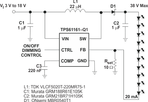 Figure 16. Typical Application of TPS61161
8.2.1.1 Design Requirements
Example requirements for white-LED-driver applications:
Table 3. Design Parameters
| DESIGN PARAMETER | EXAMPLE VALUE |
|---|---|
| Inductor | 22 µH |
| Minimum input voltage | 3 V |
| Number of series LED | 10 |
| LED maximum forward voltage (Vf) | 3.2 V |
| Schottky diode forward voltage (Vf) | 0.2 V |
| Efficiency (η) | 85% |
| Switching frequency (SW) | 600 kHz |
Applying Equation 3 and Equation 4, when VIN is 3 V, 10 LEDs output equivalent to VOUT of 32.2 V, the inductor is 22 μH, the Schottky forward voltage is 0.2 V, the maximum output current is 47 mA in typical condition.
8.2.1.2 Detailed Design Procedure
8.2.1.2.1 Maximum Output Current
The overcurrent limit in a boost converter limits the maximum input current and thus maximum input power for a given input voltage. Maximum output power is less than maximum input power due to power conversion losses. Therefore, the current limit setting, input voltage, output voltage and efficiency can all change maximum current output. The current limit clamps the peak inductor current; therefore, the ripple has to be subtracted to derive maximum DC current. The ripple current is a function of switching frequency, inductor value and duty cycle. Equation 3 and Equation 4 take into account of all the above factors for maximum output current calculation.

where
- Ip = inductor peak-to-peak ripple
- L = inductor value
- Vf = Schottky diode forward voltage
- Fs = switching frequency
- Vout = output voltage of the boost converter. It is equal to the sum of VFB and the voltage drop across LEDs.

where
- Iout_max = maximum output current of the boost converter
- Ilim = overcurrent limit
- η = efficiency
For instance, when VIN is 3 V, 8 LEDs output equivalent to VOUT of 26 V, the inductor is 22 μH, the Schottky forward voltage is 0.2 V; and then the maximum output current is 65 mA in typical condition. When VIN is 5 V, 10 LEDs output equivalent to VOUT of 32 V, the inductor is 22 μH, the Schottky forward voltage is 0.2 V; and then the maximum output current is 85 mA in typical condition.
8.2.1.2.2 Inductor Selection
The selection of the inductor affects steady state operation as well as transient behavior and loop stability. These factors make it the most important component in power regulator design. There are three important inductor specifications, inductor value, DC resistance and saturation current. Considering inductor value alone is not enough.
The inductor value determines the inductor ripple current. Choose an inductor that can handle the necessary peak current without saturating, according to half of the peak-to-peak ripple current given by Equation 3, pause the inductor DC current given by:

Inductor values can have ±20% tolerance with no current bias. When the inductor current approaches saturation level, its inductance can decrease 20% to 35% from the 0A value depending on how the inductor vendor defines saturation current. Using an inductor with a smaller inductance value forces discontinuous PWM when the inductor current ramps down to zero before the end of each switching cycle. This reduces the boost converter’s maximum output current, causes large input voltage ripple and reduces efficiency. Large inductance value provides much more output current and higher conversion efficiency. For these reasons, a 10-μH to 22-μH inductor value range is recommended. A 22-μH inductor optimized the efficiency for most application while maintaining low inductor peak-to-peak ripple. Table 4 lists the recommended inductor for the TPS61160 or TPS61161. When recommending inductor value, the factory has considered –40% and 20% tolerance from its nominal value.
The TPS61160 and TPS61161 have built-in slope compensation to avoid sub-harmonic oscillation associated with current mode control. If the inductor value is lower than 10 μH, the slope compensation may not be adequate, and the loop can be unstable. Therefore, customers need to verify the inductor in their application if it is different from the recommended values.
Table 4. Recommended Inductors for TPS61160 and TPS61161
| PART NUMBER | L (μH) | DCR MAX (Ω) | SATURATION CURRENT (mA) | SIZE (L × W × H mm) |
VENDOR |
|---|---|---|---|---|---|
| LQH3NPN100NM0 | 10 | 0.3 | 750 | 3 ×3 ×1.5 | Murata |
| VLCF5020T-220MR75-1 | 22 | 0.4 | 750 | 5 ×5 × 2.0 | TDK |
| CDH3809/SLD | 10 | 0.3 | 570 | 4 × 4 × 1.0 | Sumida |
| A997AS-220M | 22 | 0.4 | 510 | 4 × 4 × 1.8 | TOKO |
8.2.1.2.3 Schottky Diode Selection
The high switching frequency of the TPS61160, TPS61161 demands a high-speed rectification for optimum efficiency. Ensure that the diode average and peak current rating exceeds the average output current and peak inductor current. In addition, the diode’s reverse breakdown voltage must exceed the open LED protection voltage. The ONSemi MBR0540 and the ZETEX ZHCS400 are recommended for TPS61160 and TPS61161.
8.2.1.2.4 Compensation Capacitor Selection
The compensation capacitor C3 (see the Functional Block Diagram), connected from COMP pin to GND, is used to stabilize the feedback loop of the TPS61160, TPS61161. A 220-nF ceramic capacitor for C3 is suitable for most applications.
8.2.1.2.5 Input and Output Capacitor Selection
The output capacitor is mainly selected to meet the requirements for the output ripple and loop stability. This ripple voltage is related to the capacitor’s capacitance and its equivalent series resistance (ESR). Assuming a capacitor with zero ESR, the minimum capacitance needed for a given ripple can be calculated by:

where
- Vripple = peak-to-peak output ripple
The additional output ripple component caused by ESR is calculated using:

Due to its low ESR, Vripple_ESR can be neglected for ceramic capacitors, but must be considered if tantalum or electrolytic capacitors are used.
Care must be taken when evaluating a ceramic capacitor’s derating under DC bias, aging and AC signal. For example, larger form factor capacitors (in 1206 size) have a resonant frequencies in the range of the switching frequency. So the effective capacitance is significantly lower. The DC bias can also significantly reduce capacitance. Ceramic capacitors can loss as much as 50% of its capacitance at its rated voltage. Therefore, leave the margin on the voltage rating to ensure adequate capacitance at the required output voltage.
The capacitor in the range of 1 μF to 4.7 μF is recommended for input side. The output requires a capacitor in the range of 0.47 μF to 10 μF. The output capacitor affects the loop stability of the boost regulator. If the output capacitor is below the range, the boost regulator can potentially become unstable. For example, when using an output capacitor of 0.1 μF, a 470-nF compensation capacitor has to be used for the loop stable.
The popular vendors for high value ceramic capacitors are:
TDK (http://www.component.tdk.com/components.php)
Murata (http://www.murata.com/cap/index.html)
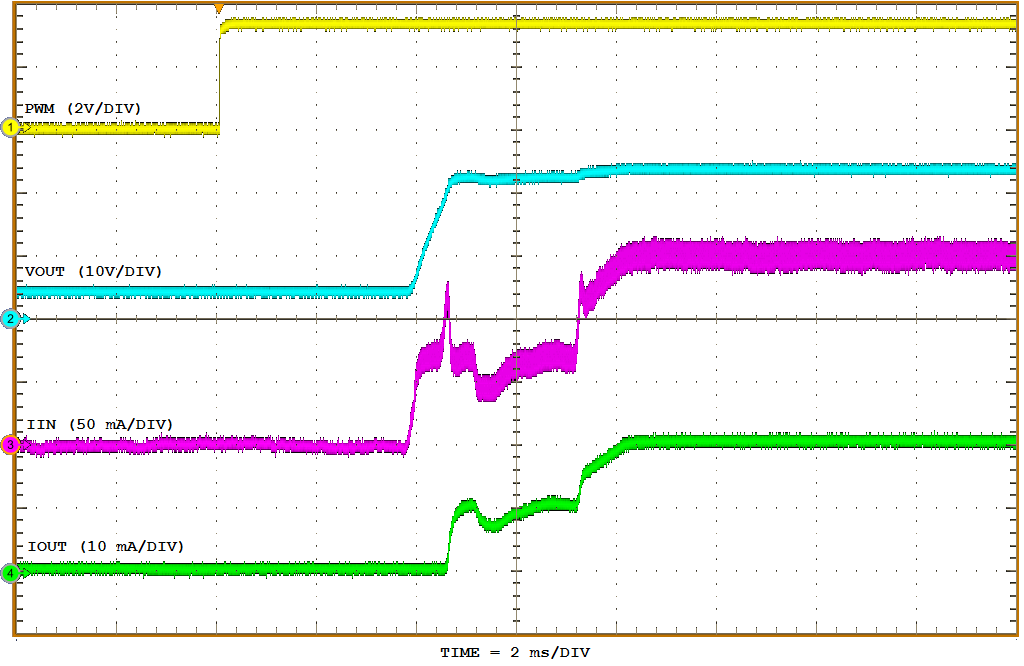
8.2.1.3 Application Curves
8.2.2 Li-Ion Driver for 6 White LEDs with External PWM Dimming Network
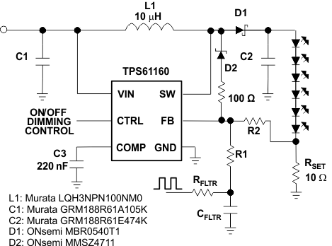 Figure 19. Li-Ion Driver for 6 White LEDs with External PWM Dimming
8.2.2.1 Design Requirements
Example parameters for white LEDs with external PWM dimming:
Table 5. Design Parameters for White LEDs with External PWM Dimming
| DESIGN PARAMETER | EXAMPLE VALUE |
|---|---|
| Inductor | 10 µH |
| Minimum input voltage | 3.6 V |
| Number of series LED | 6 |
| LED maximum forward voltage (Vf) | 3.2 V |
| Schottky diode forward voltage (Vf) | 0.2 V |
| Efficiency | 90% |
| Switching frequency (fSW) | 600 kHz |
| External PWM output voltage | 3 V |
| External PWM frequency | 20 kHz |
Applying Equation 3 and Equation 4 when VIN is 3 V, 6 LEDs output equivalent to VOUT of 19.4 V, the inductor is 10 μH, the Schottky forward voltage is 0.2 V, the maximum output current is 76 mA in typical condition.
8.2.2.2 Detailed Design Procedure
8.2.2.2.1 Choosing Component Values
As per SLVA471, the values of RFLTR, CFLTR, R1, R2, and RSET are determined by the system parameters and error tolerance. The main source of LED current error is leakage current from the FB pin. The error gets worse as the LED current decreases. The error due to leakage current is given by Functional Block Diagram, where the impedance seen by the FB pin has a major impact. To reduce error due to the leakage current, the impedance seen by the FB pin needs to be small. Because R2 is much smaller than R1 + RFLTR, R2 must be chosen to be small to minimize the impedance seen by the FB pin. In general, R2 must be chosen to be 1 kΩ or less. If greater accuracy at smaller currents is needed, then R2 must be chosen to be even smaller.

Once R2 has been chosen, the value of RSET and R1 + RFLTR can be calculated using Equation 9, Equation 10, Equation 11, and Equation 12. The individual values of R1 and RFLTR can be any combination that sums up to R1 + RFLTR . In general, choosing R1 and RFLTR to be the same value gives a minimum requirement for CFLTR.


Finally, CFLTR can be chosen based on the amount of filtering desired or to provide a gradual dimming effect that is popular in many lighting products. At a minimum, CFLTR must be chosen to provide at least 20 dB of attenuation at the PWM frequency. Equation 13 can be used to calculate the minimum capacitor value to provide this attenuation.

To provide gradual dimming, a large capacitor must be chosen to provide a long transient time when changing the PWM duty cycle. Equation 14 shows how to calculate the recommended corner frequency of the RC filter based on the 10% to 90% rise time. Once the corner frequency is known, it can be used to calculate the required capacitor using Equation 15.


For example, a design with RFLTR and R1 equal to 10 kΩ and a desired rise time of 500 ms requires a corner frequency of 0.7 Hz and a capacitor of 47 μF.
8.2.2.3 Application Curves
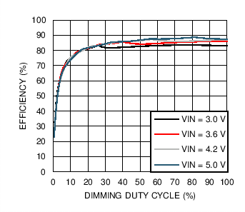
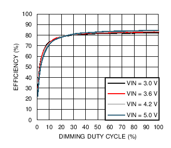 Figure 20. Efficiency vs Dimming Duty Cycle
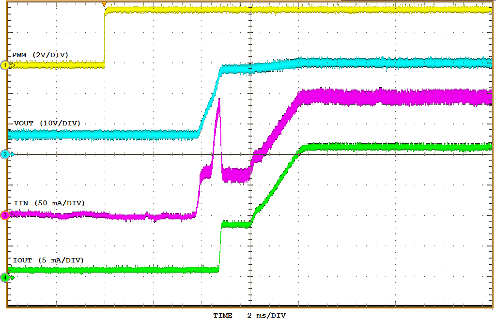
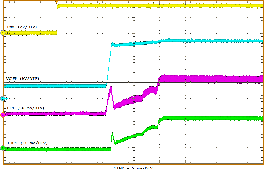 Figure 22. Start-Up with 6 Series LEDs (External PWM, DPWM = 100%)
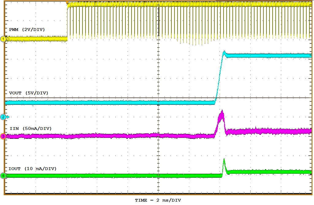
8.2.3 Li-Ion Driver for 6 White LEDs
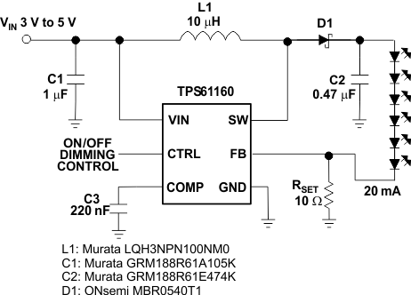 Figure 23. Li-Ion Driver for 6 White LEDs
8.2.3.1 Design Requirements
Example parameters for Li-Ion drivers with 6 white LEDs:
Table 6. Design Parameters for Li-Ion Driver with 6 White LEDs
| DESIGN PARAMETER | EXAMPLE VALUE |
|---|---|
| Inductor | 10 µH |
| Minimum input voltage | 3 V |
| Number of series LED | 6 |
| LED maximum forward voltage (Vf) | 3.2 V |
| Schottky diode forward voltage (Vf) | 0.6 V |
| Efficiency (η) | 88% |
| Switching frequency | 600 kHz |
Applying Equation 3 and Equation 4, when VIN is 3 V, 6 LEDs output equivalent to VOUT of 19.4 V, the inductor is 10 μH, the Schottky forward voltage is 0.2 V, the maximum output current is 66 mA in typical condition.
8.2.3.2 Detailed Design Procedure
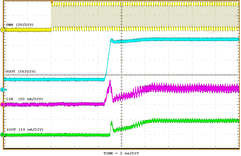
8.2.3.3 Application Curves
 Figure 24. Efficiency vs Duty Cycle
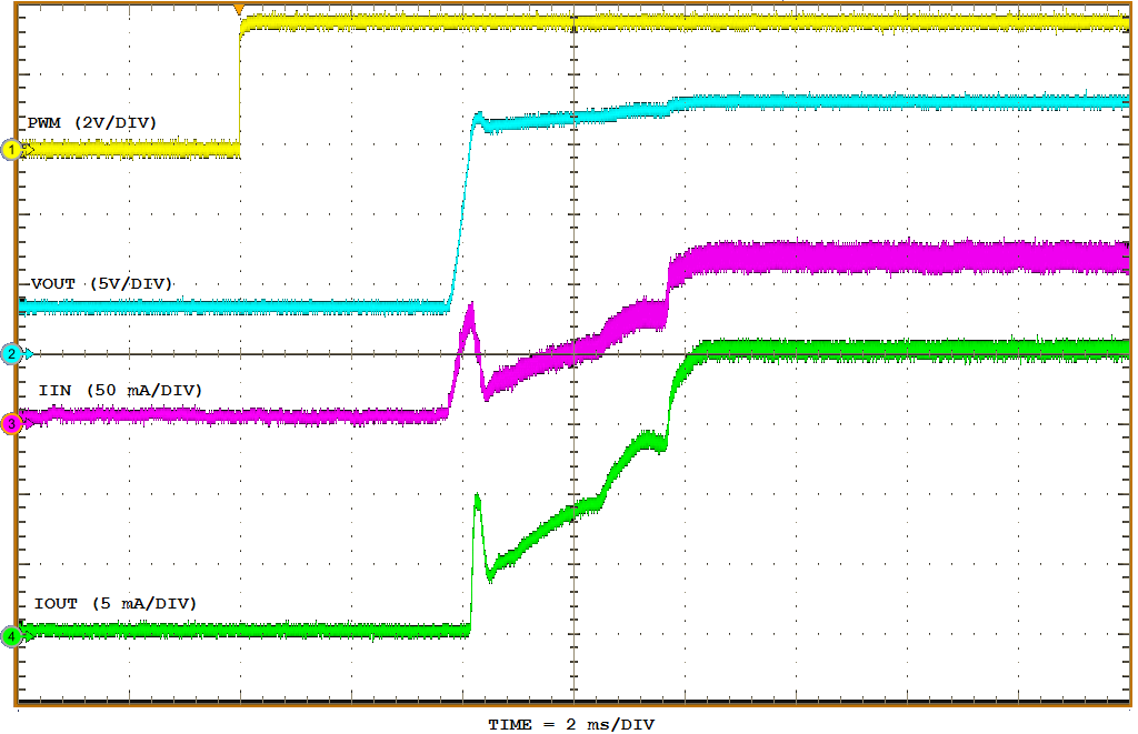 Figure 26. Start-Up with 6 Series LEDs (DPWM = 100%)
8.2.4 Li-Ion Driver for 8 White LEDs
For assistance in selecting the proper values for RSET, R1-R3, RFLTR, CFLTR and D2 for the specific application, refer to SLVA471 and/or SLVC366.
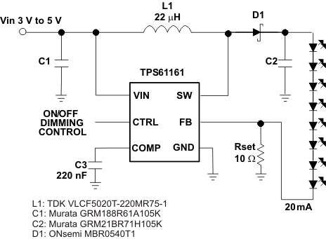 Figure 27. Li-Ion Driver for 8 White LEDs
8.2.4.1 Design Requirements
Example parameters for Li-Ion driver with 8 white LEDs:
Table 7. Design Parameters for Li-Ion Driver with 8 White LEDs
| DESIGN PARAMETER | EXAMPLE VALUE |
|---|---|
| Inductor | 22 µH |
| Minimum input voltage | 3 V |
| Number of series LED | 8 |
| LED maximum forward voltage (Vf) | 3.2 V |
| Schottky diode forward voltage | 0.2 V |
| Efficiency (η) | 85% |
| Switching frequency | 600 kHz |
Applying Equation 3 and Equation 4, when VIN is 3 V, 8 LEDs output equivalent to VOUT of 25.8 V, the inductor is 22 μH, the Schottky forward voltage is 0.2 V, the maximum output current is 60 mA in typical condition.
8.2.4.2 Detailed Design Procedure
8.2.4.3 Application Curves
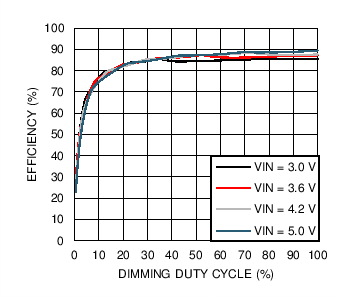 Figure 28. Efficiency vs Duty Cycle
