SLVS859B June   2008  – December 2014 TPS61085

PRODUCTION DATA.  

  1. Features
  2. Applications
  3. Description
  4. Simplified Schematic
  5. Revision History
  6. Pin Configuration and Functions
  7. Specifications
    1. 7.1 Absolute Maximum Ratings
    2. 7.2 ESD Ratings
    3. 7.3 Recommended Operating Conditions
    4. 7.4 Thermal Information
    5. 7.5 Electrical Characteristics
    6. 7.6 Typical Characteristics
  8. Detailed Description
    1. 8.1 Overview
    2. 8.2 Functional Block Diagram
    3. 8.3 Feature Description
      1. 8.3.1 Soft-Start
      2. 8.3.2 Frequency Select Pin (FREQ)
      3. 8.3.3 Undervoltage Lockout (UVLO)
      4. 8.3.4 Thermal Shutdown
      5. 8.3.5 Overvoltage Prevention
    4. 8.4 Device Functional Modes
  9. Application and Implementation
    1. 9.1 Application Information
    2. 9.2 Typical Application
      1. 9.2.1 Design Requirements
      2. 9.2.2 Detailed Design Procedure
        1. 9.2.2.1 Design Procedure
        2. 9.2.2.2 Inductor Selection
        3. 9.2.2.3 Rectifier Diode Selection
        4. 9.2.2.4 Setting the Output Voltage
        5. 9.2.2.5 Compensation (COMP)
        6. 9.2.2.6 Input Capacitor Selection
        7. 9.2.2.7 Output Capacitor Selection
      3. 9.2.3 Application Curves
    3. 9.3 System Examples
      1. 9.3.1 General Boost Application Circuits
      2. 9.3.2 TFT LCD Application Circuit
      3. 9.3.3 WHITE LED Application Circuits
  10. 10Power Supply Recommendations
  11. 11Layout
    1. 11.1 Layout Guidelines
    2. 11.2 Layout Example
  12. 12Device and Documentation Support
    1. 12.1 Trademarks
    2. 12.2 Electrostatic Discharge Caution
    3. 12.3 Glossary
  13. 13Mechanical, Packaging, and Orderable Information

封装选项

机械数据 (封装 | 引脚)
散热焊盘机械数据 (封装 | 引脚)
订购信息

6 Pin Configuration and Functions

DGK, PW Packages
8 Pins
Top View
po_lvs859.gif
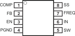
8-PIN 4.9-mm × 3-mm × 1.1-mm VSSOP (DGK)
8-PIN 6.4-mm × 3-mm × 1.2-mm TSSOP (PW)

Pin Functions

PIN I/O DESCRIPTION
NAME NO.
COMP 1 I/O Compensation pin
EN 3 I Shutdown control input. Connect this pin to logic high level to enable the device
FB 2 I Feedback pin
FREQ 7 I Frequency select pin. The power switch operates at 650 kHz if FREQ is connected to GND and at 1.2 MHz if FREQ is connected to IN
IN 6 I Input supply pin
PGND 4 Power ground
SS 8 O Soft-start control pin. Connect a capacitor to this pin if soft-start needed. Open = no soft-start
SW 5 I Switch pin