ZHCSFA0 June   2016 TPS61021A

PRODUCTION DATA.  

  1. 特性
  2. 应用
  3. 说明
  4. 修订历史记录
  5. Pin Configuration and Functions
  6. Specifications
    1. 6.1 Absolute Maximum Ratings
    2. 6.2 ESD Ratings
    3. 6.3 Recommended Operating Conditions
    4. 6.4 Thermal Information
    5. 6.5 Electrical Characteristics
    6. 6.6 Typical Characteristics
  7. Detailed Description
    1. 7.1 Overview
    2. 7.2 Functional Block Diagram
    3. 7.3 Feature Description
      1. 7.3.1 Under-Voltage Lockout
      2. 7.3.2 Enable and Soft Start
      3. 7.3.3 Switching Frequency
      4. 7.3.4 Current Limit Operation
      5. 7.3.5 Pass-Through Operation
      6. 7.3.6 Over-Voltage Protection
      7. 7.3.7 Output Short-to-Ground Protection
      8. 7.3.8 Thermal Shutdown
    4. 7.4 Device Functional Modes
      1. 7.4.1 PWM Mode
      2. 7.4.2 Power Save Mode
  8. Application and Implementation
    1. 8.1 Application Information
    2. 8.2 Typical Application
      1. 8.2.1 Design Requirements
      2. 8.2.2 Detailed Design Procedure
        1. 8.2.2.1 Setting the Output Voltage
        2. 8.2.2.2 Inductor Selection
        3. 8.2.2.3 Output Capacitor Selection
        4. 8.2.2.4 Feedforward Capacitor Selection
        5. 8.2.2.5 Input Capacitor Selection
      3. 8.2.3 Application Curves
  9. Power Supply Recommendations
  10. 10Layout
    1. 10.1 Layout Guidelines
    2. 10.2 Layout Example
    3. 10.3 Thermal Considerations
  11. 11器件和文档支持
    1. 11.1 器件支持
      1. 11.1.1 Third-Party Products Disclaimer
    2. 11.2 社区资源
    3. 11.3 商标
    4. 11.4 静电放电警告
    5. 11.5 Glossary
  12. 12机械、封装和可订购信息
    1. 12.1 Package Option Addendum
      1. 12.1.1 Packaging Information
      2. 12.1.2 Tape and Reel Information

封装选项

机械数据 (封装 | 引脚)
散热焊盘机械数据 (封装 | 引脚)

5 Pin Configuration and Functions

DSG Package
8-Pin WSON with Thermal Pad
Top View
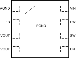
TPS61021A po_slvsd21.gif

Pin Functions

PIN I/O DESCRIPTION
NAME NO.
AGND 1 I Signal ground of the IC
FB 2 I Voltage feedback of adjustable output voltage
VOUT 3,4 PWR Boost converter output
EN 5 I Enable logic input. Logic high voltage enables the device. Logic low voltage disables the device and turns it into shutdown mode.
SW 6,7 PWR The switch pin of the converter. It is connected to the drains of the internal power MOSFETs.
VIN 8 I IC power supply input
PGND 9 PWR Power ground