SLVS372C June   2001  – October 2015 TPS60240 , TPS60241 , TPS60242 , TPS60243

PRODUCTION DATA.  

  1. Features
  2. Applications
  3. Description
  4. Revision History
  5. Pin Configuration and Functions
  6. Specifications
    1. 6.1 Absolute Maximum Ratings
    2. 6.2 ESD Ratings
    3. 6.3 Recommended Operating Conditions
    4. 6.4 Thermal Information
    5. 6.5 Electrical Characteristics
    6. 6.6 Typical Characteristics
  7. Detailed Description
    1. 7.1 Overview
    2. 7.2 Functional Block Diagram
    3. 7.3 Feature Description
      1. 7.3.1 Thermal Shutdown
      2. 7.3.2 Current Limit
    4. 7.4 Device Functional Modes
      1. 7.4.1 Start-up Procedure
      2. 7.4.2 Shutdown
  8. Application and Implementation
    1. 8.1 Application Information
    2. 8.2 Typical Applications
      1. 8.2.1 5-V Low-Noise VCO Supply from 3.3-V Input
        1. 8.2.1.1 Design Requirements
        2. 8.2.1.2 Detailed Design Procedure
          1. 8.2.1.2.1 Output Voltage Ripple
        3. 8.2.1.3 Application Curves
      2. 8.2.2 2-V to 3.3-V Low-Noise Converter
  9. Power Supply Recommendations
  10. 10Layout
    1. 10.1 Layout Guidelines
    2. 10.2 Layout Examples
  11. 11Device and Documentation Support
    1. 11.1 Device Support
      1. 11.1.1 Third-Party Products Disclaimer
    2. 11.2 Related Links
    3. 11.3 Community Resources
    4. 11.4 Trademarks
    5. 11.5 Electrostatic Discharge Caution
    6. 11.6 Glossary
  12. 12Mechanical, Packaging, and Orderable Information

封装选项

请参考 PDF 数据表获取器件具体的封装图。

机械数据 (封装 | 引脚)
  • DGK|8
散热焊盘机械数据 (封装 | 引脚)
订购信息

10 Layout

10.1 Layout Guidelines

To achieve optimal noise behavior, keep the power lines to the capacitors and load as short as possible. Use of power planes is recommended.

10.2 Layout Examples
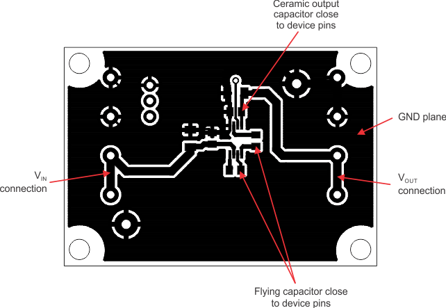
TPS60240 TPS60241 TPS60242 TPS60243 layoutexample2.gif Figure 33. Top Layer
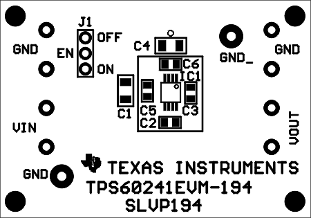
TPS60240 TPS60241 TPS60242 TPS60243 layoutexample1.gif Figure 34. Top Silkscreen