ZHCSJH9A August   2019  – August 2019 TPS56C230

PRODUCTION DATA.  

  1. 特性
  2. 应用
  3. 说明
    1.     Device Images
      1.      简化原理图
      2.      效率与输出电流 Eco-mode
  4. 修订历史记录
  5. Pin Configuration and Functions
    1.     Pin Functions
  6. Specifications
    1. 6.1 Absolute Maximum Ratings
    2. 6.2 ESD Ratings
    3. 6.3 Recommended Operating Conditions
    4. 6.4 Thermal Information
    5. 6.5 Electrical Characteristics
    6. 6.6 Typical Characteristics
  7. Detailed Description
    1. 7.1 Overview
    2. 7.2 Functional Block Diagram
    3. 7.3 Feature Description
      1. 7.3.1  PWM Operation and D-CAP3 Control
      2. 7.3.2  Soft Start
      3. 7.3.3  Large Duty Operation
      4. 7.3.4  Power Good
      5. 7.3.5  Overcurrent Protection and Undervoltage Protection
      6. 7.3.6  Overvoltage Protection
      7. 7.3.7  Out-of-Bounds Operation
      8. 7.3.8  UVLO Protection
      9. 7.3.9  Output Voltage Discharge
      10. 7.3.10 Thermal Shutdown
    4. 7.4 Device Functional Modes
      1. 7.4.1 Light Load Operation
      2. 7.4.2 Eco-mode Control
      3. 7.4.3 Force CCM
      4. 7.4.4 Mode Selection
      5. 7.4.5 Standby Operation
  8. Application and Implementation
    1. 8.1 Application Information
    2. 8.2 Typical Application
      1. 8.2.1 Design Requirements
      2. 8.2.2 Detailed Design Procedure
        1. 8.2.2.1 Custom Design With WEBENCH® Tools
        2. 8.2.2.2 Output Voltage Set Point
        3. 8.2.2.3 MODE Selection
        4. 8.2.2.4 Inductor Selection
        5. 8.2.2.5 Output Capacitor Selection
        6. 8.2.2.6 Input Capacitor Selection
      3. 8.2.3 Application Curves
  9. Power Supply Recommendations
  10. 10Layout
    1. 10.1 Layout Guidelines
    2. 10.2 Layout Example
  11. 11器件和文档支持
    1. 11.1 器件支持
      1. 11.1.1 第三方产品免责声明
      2. 11.1.2 开发支持
        1. 11.1.2.1 使用 WEBENCH® 工具创建定制设计
    2. 11.2 接收文档更新通知
    3. 11.3 社区资源
    4. 11.4 商标
    5. 11.5 静电放电警告
    6. 11.6 Glossary
  12. 12机械、封装和可订购信息

封装选项

机械数据 (封装 | 引脚)
散热焊盘机械数据 (封装 | 引脚)
订购信息

Typical Characteristics

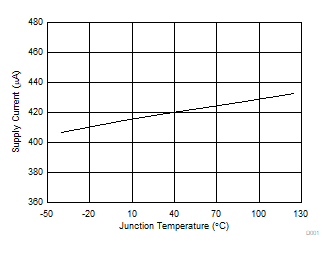
TPS56C230 D001-SupplyCurrent.gif
VEN = 5 V
Figure 1. Supply Current vs Junction Temperature
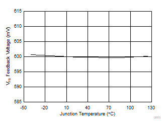
TPS56C230 D003-VFB.gif
Figure 3. Feedback Voltage vs Junction Temperature
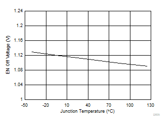
TPS56C230 D005-ENoff.gif
Figure 5. Enable Off Voltage vs Junction Temperature
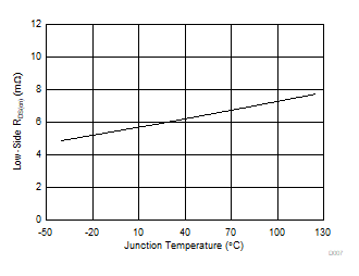
TPS56C230 D007-RDSL.gif
Figure 7. Low-Side RDS(on) vs Junction Temperature
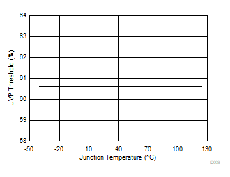
TPS56C230 D009-UVP.gif
Figure 9. UVP Threshold vs Junction Temperature
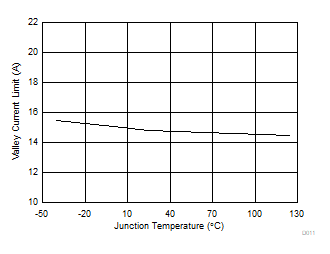
TPS56C230 D011-OC.gif
Figure 11. Valley Current Limit vs Junction Temperature
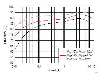
TPS56C230 D013-EfficiencyEco.gif
Figure 13. Efficiency vs Load Current, Eco-mode
TPS56C230 D017-FswEco.gif
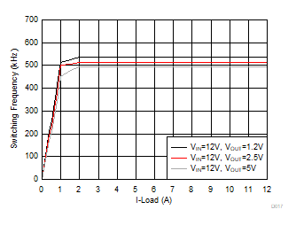
Figure 15. Switching Frequency vs Load Current, Eco-mode
TPS56C230 D002-ShutdownCurrent.gif
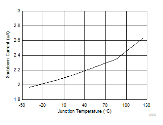
VEN = 0 V
Figure 2. Shutdown Current vs Temperature
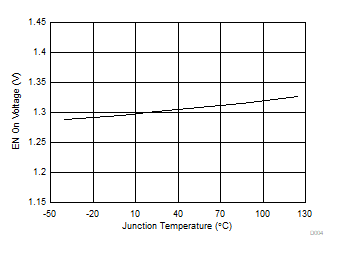
TPS56C230 D004-EN.gif
Figure 4. Enable On Voltage vs Junction Temperature
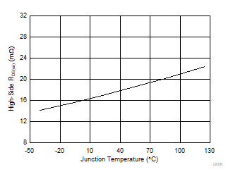
TPS56C230 D006-RDSH.gif
Figure 6. High-Side RDS(on) vs Junction Temperature
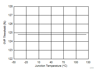
TPS56C230 D008-OVP.gif
Figure 8. OVP Threshold vs Junction Temperature
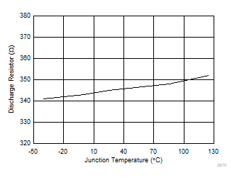
TPS56C230 D010-DischargeR.gif
Figure 10. Discharge Resistor vs Junction Temperature
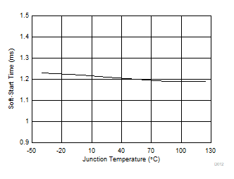
TPS56C230 D012-SSTime.gif
Figure 12. Soft-Start Time vs Junction Temperature
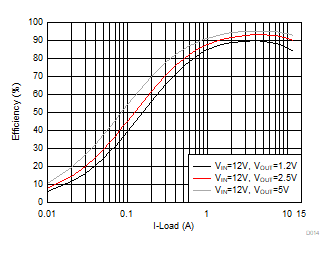
TPS56C230 D014-EfficiencyFccm.gif
Figure 14. Efficiency vs Load Current, FCCM
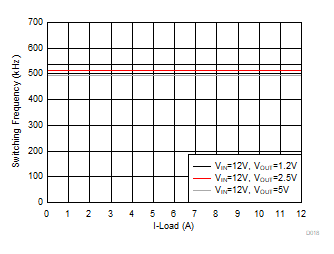
TPS56C230 D018-FswFccm.gif
Figure 16. Switching Frequency vs Load Current, FCCM