ZHCSEU8F march 2016 – august 2023 TPS56C215
PRODUCTION DATA
- 1
- 1 特性
- 2 应用
- 3 说明
- 4 Revision History
- 5 Pin Configuration and Functions
- 6 Specifications
-
7 Detailed Description
- 7.1 Overview
- 7.2 Functional Block Diagram
- 7.3
Feature Description
- 7.3.1 PWM Operation and D-CAP3 Control Mode
- 7.3.2 Eco-mode Control
- 7.3.3 4.7-V LDO
- 7.3.4 MODE Selection
- 7.3.5 Soft Start and Pre-biased Soft Start
- 7.3.6 Enable and Adjustable UVLO
- 7.3.7 Power Good
- 7.3.8 Overcurrent Protection and Undervoltage Protection
- 7.3.9 Out-of-Bounds Operation
- 7.3.10 UVLO Protection
- 7.3.11 Thermal Shutdown
- 7.3.12 Output Voltage Discharge
- 7.4 Device Functional Modes
- 8 Application and Implementation
- 9 Device and Documentation Support
- 10Mechanical, Packaging, and Orderable Information
7.3.3 4.7-V LDO
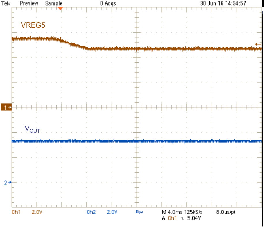
The VREG5 pin is the output of the internal 4.7-V linear regulator that creates the bias for all the internal circuitry and MOSFET gate drivers. The VREG5 pin needs to be bypassed with a 4.7-µF capacitor. An external voltage that is above the internal output voltage of the LDO can override the internal LDO, switching it to the external rail after a higher voltage is detected. This enhances the efficiency of the converter because the quiescent current now runs off this external rail instead of the input power supply. The UVLO circuit monitors the VREG5 pin voltage and disables the output when VREG5 falls below the UVLO threshold. When using an external bias on the VREG5 rail, any power-up and power-down sequencing can be applied but it is important to understand that if there is a discharge path on the VREG5 rail that can pull a current higher than the internal current limit of the LDO (ILIM5) from the VREG5, then the VREG5 LDO turns off thereby shutting down the output of TPS56C215. If such condition does not exist and if the external VREG5 rail is turned off, the VREG5 voltage switches over to the internal LDO voltage which is 4.7 V typically in a few nanoseconds. Figure 7-1 shows this transition of the VREG5 voltage from an external bias of 5.5 V to the internal LDO output of 4.7 V when the external bias to VREG5 is disabled while the output of TPS56C215 remains unchanged.
 Figure 7-1 VREG5 Transition