ZHCSIH6B July   2018  – October 2019 TPS563231

PRODUCTION DATA.  

  1. 特性
  2. 应用
  3. 说明
    1.     Device Images
      1.      简化原理图
      2.      TPS563231 效率
  4. 修订历史记录
  5. Pin Configuration and Functions
    1.     Pin Functions
  6. Specifications
    1. 6.1 Absolute Maximum Ratings
    2. 6.2 ESD Ratings
    3. 6.3 Recommended Operating Conditions
    4. 6.4 Thermal Information
    5. 6.5 Electrical Characteristics
    6. 6.6 Typical Characteristics
  7. Detailed Description
    1. 7.1 Overview
    2. 7.2 Functional Block Diagram
    3. 7.3 Feature Description
      1. 7.3.1 Adaptive On-Time Control and PWM Operation
      2. 7.3.2 Soft Start and Pre-Biased Soft Start
      3. 7.3.3 Over Current and Short Circuit Protection
      4. 7.3.4 Undervoltage Lockout (UVLO) Protection
      5. 7.3.5 Thermal Shutdown
    4. 7.4 Device Functional Modes
      1. 7.4.1 Shutdown Mode
      2. 7.4.2 Continuous Conduction Mode (CCM)
      3. 7.4.3 Pulse Skip Mode (PSM, TPS563231)
  8. Application and Implementation
    1. 8.1 Application Information
    2. 8.2 Typical Application
      1. 8.2.1 Design Requirements
      2. 8.2.2 Detailed Design Procedure
        1. 8.2.2.1 Output Voltage Resistors Selection
        2. 8.2.2.2 Output Filter Selection
        3. 8.2.2.3 Input Capacitor Selection
        4. 8.2.2.4 Bootstrap Capacitor Selection
      3. 8.2.3 Application Curves
  9. Power Supply Recommendations
  10. 10Layout
    1. 10.1 Layout Guidelines
    2. 10.2 Layout Example
  11. 11器件和文档支持
    1. 11.1 相关链接
    2. 11.2 接收文档更新通知
    3. 11.3 社区资源
    4. 11.4 商标
    5. 11.5 静电放电警告
    6. 11.6 Glossary
  12. 12机械、封装和可订购信息

封装选项

机械数据 (封装 | 引脚)
散热焊盘机械数据 (封装 | 引脚)
订购信息

Pin Configuration and Functions

DRL Package
6-Pin SOT563
Top View
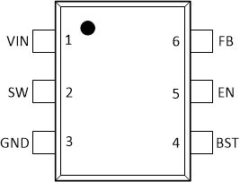
TPS563231 pinout-01-drl-pkg-slusd65.gif

Pin Functions

PIN I/O DESCRIPTION
NAME NO.
BST 4 O Supply input for the high-side NFET gate drive circuit. Connect 0.1 µF capacitor between BST and SW pins.
EN 5 I Enable input control. High = On, Low = Off. Can be connected to VIN. Do not float. Adjust the input undervoltage lockout with EN resistor divider.
FB 6 I Converter feedback input. Connect to output voltage with feedback resistor divider.
GND 3 Power ground terminals, connected to the source of low-side FET internally. Connect to system ground, ground side of CIN and COUT. Path to CIN must as short as possible.
SW 2 O Switch node connection between high-side NFET and low-side NFET.
VIN 1 I Input voltage supply pin. The drain terminal of high-side power NFET.