ZHCSG73A April 2017 – September 2020 TPS561201 , TPS561208
PRODUCTION DATA
- 1 特性
- 2 应用
- 3 说明
- 4 Revision History
- 5 Pin Configuration and Functions
- 6 Specifications
- 7 Detailed Description
- 8 Application and Implementation
- 9 Power Supply Recommendations
- 10Layout
- 11Device and Documentation Support
- 12Mechanical, Packaging, and Orderable Information
8.2.3 Application Curves
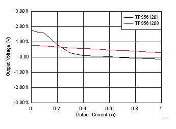 Figure 8-2 Load
Regulation VIN = 5 V
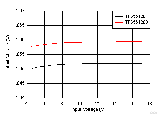
| TPS56201 IOUT = 0.5 A | TPS56208 IOUT = 10 mA |
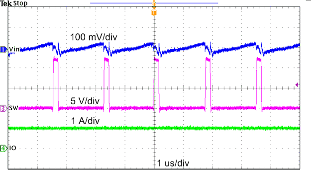 Figure 8-6 TPS561201 Input Voltage Ripple
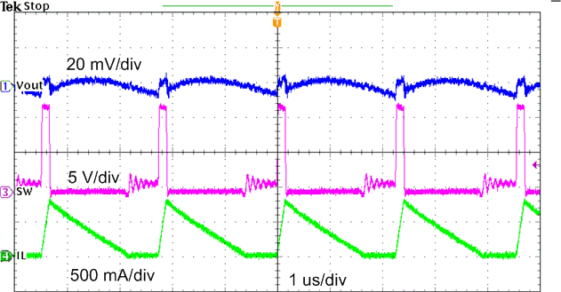 Figure 8-8 TPS561201 Output Voltage Ripple, IOUT = 0.25 A
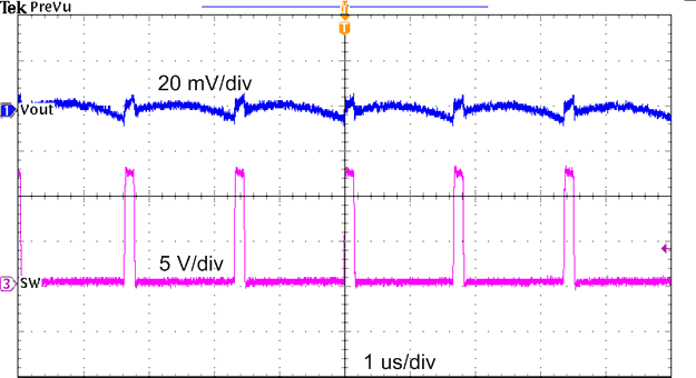 Figure 8-10 TPS561208 Output Voltage Ripple, IOUT = 0 A
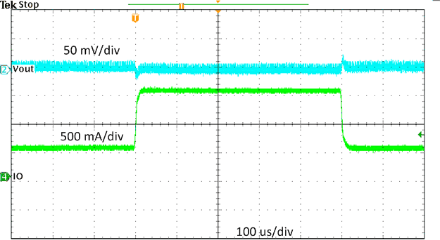 Figure 8-12 TPS561201 Transient Response, 0.5 to 1.5 A
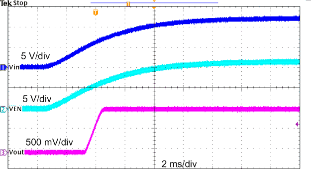 Figure 8-14 TPS561201 Start-Up Relative to VI
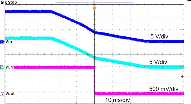 Figure 8-16 TPS561201 Shutdown Relative to VI
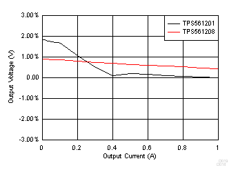 Figure 8-3 Load
Regulation VIN = 12 V
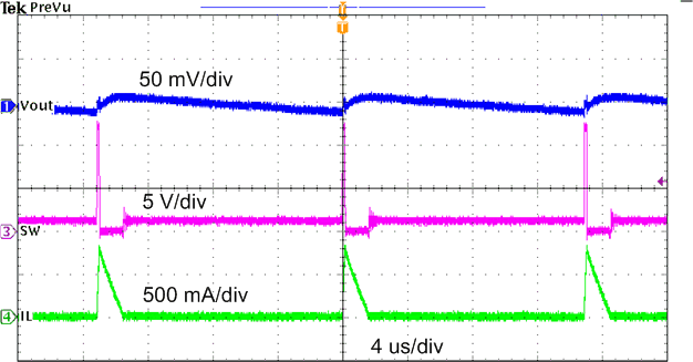 Figure 8-7 TPS561201 Output Voltage Ripple, IOUT = 10 mA
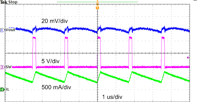 Figure 8-9 TPS561201 Output Voltage Ripple, IOUT = 1 A
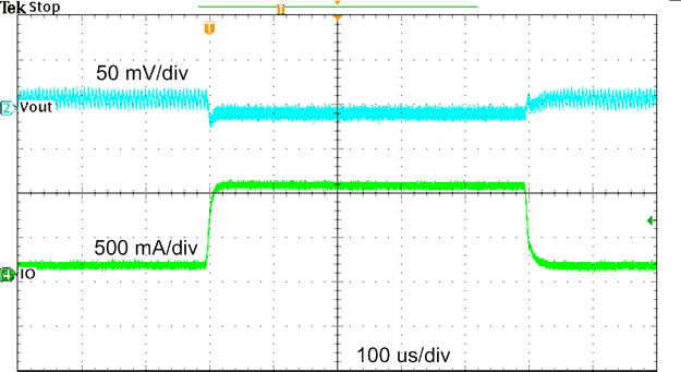 Figure 8-11 TPS561201 Transient Response, 0.1 to 1 A
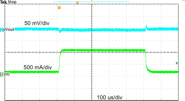 Figure 8-13 TPS561208 Transient Response 0.1 to 1 A
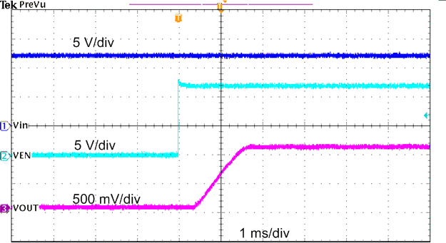 Figure 8-15 TPS561201 Start-Up Relative to EN
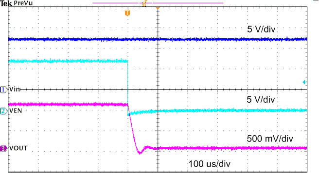 Figure 8-17 TPS561201 Shutdown Relative to EN