ZHCSEW7A December 2015 – April 2016 TPS54A20
PRODUCTION DATA.
- 1 特性
- 2 应用
- 3 说明
- 4 修订历史记录
- 5 Pin Configuration and Functions
- 6 Specifications
-
7 Detailed Description
- 7.1 Overview
- 7.2 Functional Block Diagram
- 7.3
Feature Description
- 7.3.1 Frequency Selection
- 7.3.2 External Clock Syncronization
- 7.3.3 Adjusting the Output Voltage
- 7.3.4 Soft Start
- 7.3.5 Startup into Pre-biased Outputs
- 7.3.6 Power Good (PGOOD)
- 7.3.7 Overcurrent Protection
- 7.3.8 Light Load Operation
- 7.3.9 Output Undervoltage/Overvoltage Protection
- 7.3.10 Input Undervoltage/Overvoltage Lockout
- 7.3.11 Enable and Adjusting Undervoltage Lockout
- 7.3.12 Series Capacitor Monitoring
- 7.3.13 Thermal Shutdown
- 7.3.14 Phase A Power Stage
- 7.3.15 Phase B Power Stage
- 7.3.16 Internal Gate Drive Regulator
- 7.3.17 Voltage Feed Forward
- 7.3.18 Internal Oscillator
- 7.3.19 Pulse Frequency Detector
- 7.3.20 On-Time Generator
-
8 Application and Implementation
- 8.1 Application Information
- 8.2
Typical Application
- 8.2.1 Design Requirements
- 8.2.2
Detailed Design Procedure
- 8.2.2.1 Output Voltage
- 8.2.2.2 Switching Frequency
- 8.2.2.3 On-Time
- 8.2.2.4 Inductor Selection
- 8.2.2.5 Output Capacitor Selection
- 8.2.2.6 Input Capacitor Selection
- 8.2.2.7 Series Capacitor Selection
- 8.2.2.8 Soft-Start Time Selection
- 8.2.2.9 Bootstrap Capacitor Selection
- 8.2.2.10 Gate Drive Capacitor Selection
- 8.2.2.11 Under Voltage Lockout Set Point
- 8.2.2.12 Current Limit Selection
- 8.2.3 Application Curves
- 9 Power Supply Recommendations
- 10Layout
- 11器件和文档支持
- 12机械、封装和可订购信息
8 Application and Implementation
NOTE
Information in the following applications sections is not part of the TI component specification, and TI does not warrant its accuracy or completeness. TI’s customers are responsible for determining suitability of components for their purposes. Customers should validate and test their design implementation to confirm system functionality.
8.1 Application Information
The TPS54A20 is a two-phase, synchronous series capacitor buck converter optimized for small size, low voltage applications from a 12 V input rail. See (SLVA750) for a more detailed introduction to the series capacitor buck converter topology.
8.1.1 Two-Phase Series Capacitor Buck Converter Topology
The series capacitor buck converter topology uniquely merges a switched capacitor converter and a buck converter. Only one extra capacitor (the series capacitor) is needed as compared to a conventional two-phase buck converter. Advantages include automatic current balancing between the inductors (inductor current sensing and a current sharing loop are not required), lower switching losses which enable high frequency (HF) operation, and voltage step-down through the series capacitor. The on-time of both high side switches is double that of a regular buck converter. This is particularly helpful in high frequency, high conversion ratio applications. The schematic of the converter topology and the converter switch states are shown below.
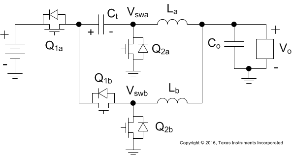 Figure 43. Two-Phase Series Capacitor Buck Converter Topology
8.1.2 Converter Switch Configurations
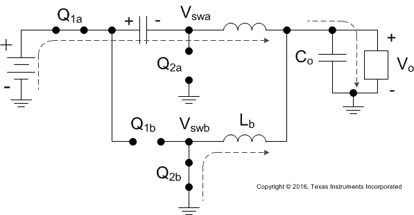 Figure 44. Phase A High Side MOSFET On
 Figure 46. Phase A/B Low Side MOSFET On
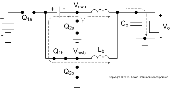 Figure 45. Phase B High Side MOSFET On
8.2 Typical Application
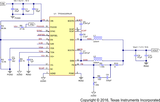 Figure 47. Typical Application
8.2.1 Design Requirements
Table 3. Design Parameters
| PARAMETER | CONDITIONS | MIN | TYP | MAX | UNIT | |
|---|---|---|---|---|---|---|
| VOUT | Output voltage | 1.2 | V | |||
| IOUT | Output current | 10 | A | |||
| ΔVOUT | Transient response | 9-A load step | 60 | mV | ||
| VIN | Input voltage | 9.2 | 12 | 14 | V | |
| VOUT(ripple) | Output voltage ripple | 20 | mV(P-P) | |||
| Start input voltage | Input voltage rising | 9.4 | V | |||
| Stop input voltage | Input voltage falling | 9.2 | V | |||
| fSW | Switching frequency | 2 | MHz | |||
| TA | Ambient temperature | 25 | °C | |||
8.2.2 Detailed Design Procedure
8.2.2.1 Output Voltage
Before beginning design, ensure that the series capacitor buck converter can be used in the application. It is recommended to use this converter when the minimum input voltage is at least five times greater than the target output voltage. If this recommendation is not followed, output voltage dropout can occur at heavy load conditions and poor transient response to load increases can result.
The output voltage is set by connecting a resistor divider network from the output voltage to the FB pin of the device and to AGND. It is recommended that the lower divider resistor maintain a range between 1 kΩ and 10 kΩ. To change the output voltage of a design, it is necessary to select the value of the upper resistor. The value of RTOP for a specific output voltage can be calculated using Equation 2.

For the example design, 1 kΩ was selected for RBOT (R7). Using Equation 2, RTOP (R9) is calculated as 1.4 kΩ. It is recommended to use resistors with ±1% or less variation.
A capacitor can be connected in parallel with the upper resistor to provide additional phase boost near the converter's crossover frequency. See (SLVA289) for more details and design guidelines. For this design, 330 pF in series with 100 Ω is used. The values were optimized based on measured loop performance.
8.2.2.2 Switching Frequency
A key design step is to decide on a switching frequency for the regulator. There is a tradeoff between higher and lower switching frequencies. Higher switching frequencies may produce a smaller solution size using lower valued inductors and smaller output capacitors compared to a power supply that switches at a lower frequency. However, the higher switching frequency creates extra switching loss, which reduces the converter’s efficiency and thermal performance. In this design, a moderate switching frequency of 2 MHz per phase is selected to achieve both a small solution size and a high efficiency operation. Refer to Table 1 for the SS/FSEL programming resistor selection.
8.2.2.3 On-Time
The TON pin requires a resistor to set the nominal on-time and to support the input voltage feedforward circuit. The resistance value used also influences the internal ramp in the controller. As a starting point, Equation 3 is recommended for selecting the TON resistor.

The RTON resistor (R5) is calculated to be 21 kΩ. The selected value for this design example is 22.1 kΩ. During startup, the converter uses the nominal on-time programmed through TON. The phase lock loop (PLL) is only activated after startup is complete. When the PLL is engaged, the on-time is adjusted. If the nominal on-time programmed through the TON pin is not close to the on-time when the PLL is engaged, the SYNC range of the device may be reduced. The TON resistor can also be adjusted to tune the controller. Lowering the RTON value will increase the internal ramp height. This will reduce the converter’s sensitivity to noise and jitter but it will also reduce the transient response capabilities of the converter.
8.2.2.4 Inductor Selection
To calculate the value of the output inductors, use Equation 4. KIND is a coefficient that represents the amount of inductor ripple current relative to the maximum output current. The inductor ripple current is filtered by the output capacitor. In general, the inductor ripple value is at the discretion of the designer; however, KIND is normally from 0.1 to 0.4 for the majority of applications.

For this design example, use KIND = 0.4 and the inductor value is calculated to be 249 nH. For this design, the nearby standard value of 220 nH was chosen. For the output filter inductor, it is generally recommended that the RMS current and saturation current ratings not be exceeded. The current ripple, RMS, and peak inductor current are calculated in Equation 5, Equation 6, and Equation 7.


For this design, the RMS inductor current is calculated to be 5.04 A and the peak inductor current is 6.13 A. The chosen inductor is 220 nH with a saturation current rating of 8.2 A and a dc current rating of 7.6 A.
The current flowing through each inductor is the inductor ripple current plus half the output current. During power up, faults, or transient load conditions, the inductor current can increase above the peak inductor current level calculated above. In transient conditions, the inductor current can increase up to the switch current limit of the device. For this reason, the most conservative approach is to specify an inductor with a saturation current rating equal to or greater than half the load current limit rather than the peak inductor current in steady state. Many inductors today have soft saturation characteristics that may be able to ride through a transient that pushes current beyond the saturation rating specified in the datasheet. An example list of inductors that have been tested to work with the TPS54A20 are shown in Table 4. Inductors not listed below can also be used with this device.
Table 4. Example Inductor List
| Inductance (nH) | Saturation Current Rating (A) | Dimensions [L x W x H] (mm) |
DCR Typ/Max (mΩ) | Type | Vendor |
|---|---|---|---|---|---|
| 220 ±20% | 9.3 | 3.2 x 2.5 x 1.2 | 9 / 12 | HMLW32251B-R22MS | CYNTEC |
| 330 ±20% | 7.5 | 3.2 x 2.5 x 1.2 | 13 / 16 | HMLW32251B-R33MS | CYNTEC |
| 220 ±30% | 8.2 | 3.2 x 2.5 x 1.2 | 7.5 / 10.5 | MLA-FY12NR22N-M3 | MAGLAYERS |
| 330 ±30% | 7.5 | 3.2 x 2.5 x 1.2 | 13.5 / 16 | MLA-FY12NR33N-M3 | MAGLAYERS |
| 220 ±20% | 8.7 | 3.2 x 2.5 x 1.2 | 9.4 / 11.6 | MCMK3225TR22MG | TAIYO YUDEN |
| 330 ±20% | 10.4 | 3.2 x 2.5 x 1.2 | 11.2 / 13.8 | MCMK3225TR33MG | TAIYO YUDEN |
| 250 ±30% | 12 | 3.2 x 2.5 x 1.5 | 10 / 12.5 | 74479290125 | WURTH ELECTRONIK |
| 330 ±30% | 12.4 | 4.1 x 4.1 x 2.1 | 6 / 7.2 | 744383560033 | WURTH ELECTRONIK |
| 220 ±20% | 10.1 | 3.5 x 3.2 x 1.5 | 7.8 / 8.9 | XEL3515-221 | COILCRAFT |
| 350 ±20% | 8.2 | 3.5 x 3.2 x 1.5 | 11.6 / 13.4 | XEL3515-351 | COILCRAFT |
| 330 ±20% | 8.5 | 2.5 x 2.0 x 1.2 | 14 / 19 | DFE252012F-R33M | TOKO |
8.2.2.5 Output Capacitor Selection
For most applications, the primary consideration for selecting the value of the output capacitor is how the regulator responds to a large change in load current. The output capacitance may also be selected based on output voltage ripple or closed-loop bandwidth design objectives.
The output capacitance required to maintain an output voltage ripple ΔVOUT during steady-state operation can be estimated using Equation 8.

The desired response to a large change in the load current is typically the most stringent criteria. The output capacitor needs to supply the load with current when the regulator cannot. This situation would occur if there are desired hold-up times for the regulator where the output capacitor must hold the output voltage above a certain level for a specified amount of time after the input power is removed. The regulator is also temporarily not able to supply sufficient output current if there is a large, fast change in the load current such as a transition from no load to full load. The output capacitor must be sized to supply the extra current to the load until the control loop responds to the load change. The minimum output capacitance required for a load increase can be estimated using Equation 9.

In low voltage applications, the inductor slew rate during a load step decrease is sometimes slower than its slew rate during a load step increase. The minimum output capacitance required for a load decrease can be estimated using Equation 10 for a given tolerable amount of overshoot in the output voltage.

Here ΔIOUT is the change in output current and ΔVOUT is the allowable change in the output voltage. For this design example, the transient load response is specified as a 3% change in VOUT for a load step of 5A. For this example, ΔIOUT = 5 A and ΔVOUT = 0.03 x 1.2 = 0.036 V. Based on these design parameters, a minimum capacitance of 93 µF is calculated using Equation 9. This value does not take the ESR of the output capacitor into account in the output voltage change. For ceramic capacitors, the ESR is usually small enough to ignore in this calculation. Additional capacitance de-ratings for aging, temperature and DC bias should be factored in which also increases this minimum value. For this design example, two 47 µF, 6.3 V rated, ceramic capacitors with 3 mΩ of ESR are selected.
8.2.2.6 Input Capacitor Selection
The TPS54A20 requires a high quality ceramic, type X5R or X7R, input decoupling capacitor of at least 4.7 µF of effective capacitance on the VIN input voltage pin. Additional bulk capacitance may also be required for the VIN input. The value of a ceramic capacitor varies significantly over temperature and the amount of DC bias applied to the capacitor. The capacitance variations due to temperature can be minimized by selecting a dielectric material that is stable over temperature. X5R and X7R ceramic dielectrics are usually selected for power regulator capacitors because they have a high capacitance to volume ratio and are fairly stable over temperature. The capacitor must also be selected with the DC bias taken into account. The capacitance value of a capacitor decreases as the DC bias across a capacitor increases. For this example design, a ceramic capacitor with at least a 25-V voltage rating is selected to support the maximum input voltage. The input capacitance value impacts the input ripple voltage of the regulator. The minimum input capacitance can be estimated using Equation 11.

Here ΔVIN is the input voltage ripple in steady state. Using the design example values, IOUT = 10 A, VOUT = 1.2 V, VIN(MIN) = 9 V, FSW = 2 MHz and ΔVIN = 25 mV, Equation 11 yields an input capacitance of 39 µF. For this example, two 10µF, 25-V and a single 22-µF, 25-V ceramic capacitors in parallel have been selected for the VIN voltage rail. Because ESR is typically fairly low in ceramic capacitors, it is not included in this calculation.
The capacitor must also have a ripple current rating greater than the maximum input current ripple to the device during full load. The input ripple current can be calculated using Equation 12.

For this example design, the RMS input ripple current is 2.21 A (RMS). The ripple current can be assumed to be shared equally between the input capacitors.
8.2.2.7 Series Capacitor Selection
A major function of the series capacitor is energy transfer. This is a different role from input and output capacitors where decoupling is the primary function. In many ways, the series capacitor is similar to the capacitor used for energy transfer in SEPIC converters and can be designed accordingly. A design objective may be to ensure the series capacitor voltage ripple does not exceed 5% to 10% of the nominal voltage under the worst case conditions. The series capacitor voltage ripple is given by Equation 13.

Here Ct is the series capacitance. Equation 13 can be rearranged to provide the design equation for series capacitor selection which is

where kCt represents the voltage ripple percentage. For example, if the voltage ripple target is 5%, the value for kCt is 0.05. The largest voltage ripple occurs at full load current (highest IOUT), highest duty ratio (lowest input voltage/highest output voltage), and lowest frequency. For this design example, the value for kCt was selected to be 0.08. The resulting series capacitance calculated is 1.85 µF. A 10 V, X7R ceramic capacitor with 2.2 µF of capacitance is selected.
Another aspect to consider is capacitor RMS current rating. This impacts the temperature rise of the capacitor. Check the capacitor datasheet for temperature rise information. If the temperature rise is too large for a single capacitor, multiple capacitors may be placed in parallel to share the RMS current. The series capacitor has the same current profile as the high side MOSFETs. The RMS current squared can be expressed as

where IL(RMS) is the RMS inductor current of either inductor. The series capacitor RMS current can be expressed as

where ΔIL is the inductor current ripple. The largest RMS current occurs at the highest load current and highest duty ratio.
Multilayer ceramic capacitors (MLCC) are well suited for operating as the series capacitor. The equivalent series resistance (ESR) is relatively low (for example, 5 mΩ to 10 mΩ) which helps to reduce power loss and self heating. The equivalent series inductance (ESL) is fairly low which results in a high self resonant frequency (SRF). There are a few key items that should be considered when designing. First, the effective capacitance decreases with DC bias. This means that the capacitor should be selected based on its capacitance with the nominal voltage of VIN/2 applied. Temperature variation also reduces effective capacitance. For this reason, X7R capacitors with up to 125°C operating temperature range are recommended. If capacitors are not properly selected, cracking or other failure modes may result.
8.2.2.8 Soft-Start Time Selection
The soft-start time is the amount of time it takes for the output voltage to reach its nominal programmed value during power up. This is useful if a load requires a controlled voltage slew rate. This is also used if the output capacitance is very large and would require large amounts of current to quickly charge the capacitor to the desired output voltage level. The large currents necessary to charge the capacitor may make the TPS54A20 reach the current limit and trigger a fault. Excessive current draw from the input power supply may cause the input voltage rail to sag. Limiting the output voltage slew rate solves both of these problems. The soft-start time can be selected using the resistor values listed in Table 1. For the example circuit, the soft-start time is not critical since the output capacitor value is 94 µF which does not require a large amount of current to charge to 1.2 V. For this example design, the average output current is approximately 220 mA during soft start. The example circuit has the soft start time set to 512 µs which requires no resistor (open connection) on the SS/FSEL pin. The average converter output current required to charge the output capacitors to the target output voltage during soft start can be estimated using Equation 17.

8.2.2.9 Bootstrap Capacitor Selection
A 0.047 μF ceramic capacitor should be connected between the BOOTA to SCAP pins and between the BOOTB and SWB pins for proper operation. It is recommended to use a ceramic capacitor with X5R or better grade dielectric. The capacitor should have 10 V or higher voltage rating.
8.2.2.10 Gate Drive Capacitor Selection
A 1 μF ceramic capacitor should be connected between VGA and PGND and between the VG+ and VG- pins for proper operation. It is recommended to use a ceramic capacitor with X5R or better grade dielectric. The VGA capacitor should have 16 V or higher voltage rating and the VG+ capacitor should have 10 V or higher voltage rating.
8.2.2.11 Under Voltage Lockout Set Point
The Under Voltage Lock Out (UVLO) set point can be adjusted using an external voltage divider network. The top resistor is connected between VIN and the EN pin and bottom resistor is connected between EN and GND as shown in Figure 42. For the example design, the supply should turn on and start switching once the input voltage increases above 9.4 V (UVLO start or enable). After the regulator starts switching, it should continue to do so until the input voltage falls below 9.2 V (UVLO stop or disable). The resistor values for obtaining the desired UVLO thresholds can be calculated using Equation 18 and Equation 19. REN,TOP, the top UVLO divider resistor, is calculated using Equation 18. REN,BOT, the bottom UVLO divider resistor, is calculated in Equation 19.


For the start and stop voltages specified the resistor value selected for REN,TOP (R2) is 80.6 kΩ and for REN,BOT (R3) is 12.4 kΩ.
8.2.2.12 Current Limit Selection
The current limit can be selected using the ILIM pin. Refer to Table 2 for resistor selection information. It is recommended to choose a current limit that is 1.5 times or more than the full load current expected in the application. This allows for margin in the inductor currents when responding to load transients and limits nuisance trips.
8.2.3 Application Curves
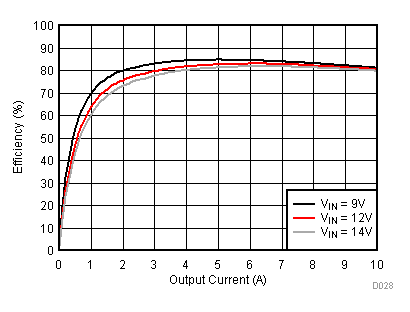 Figure 48. Efficiency
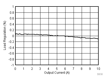 Figure 50. Load Regulation
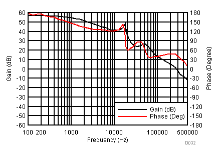 Figure 52. Loop Response
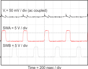 Figure 54. No Load Input Voltage Ripple
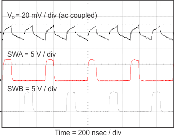 Figure 56. No Load Output Voltage Ripple
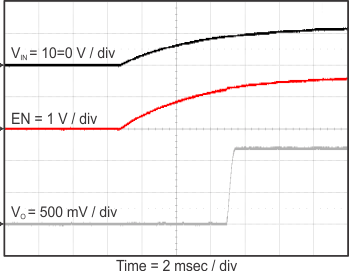 Figure 58. Start Up with VIN
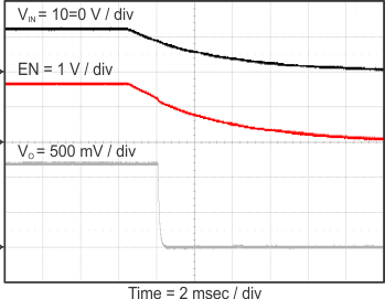 Figure 60. Shut Down with VIN
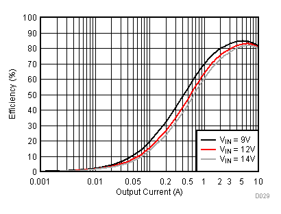 Figure 49. Light Load Efficiency
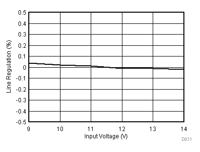 Figure 51. Line Regulation
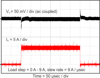 Figure 53. Transient Response
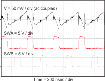 Figure 55. Full Load Input Voltage Ripple
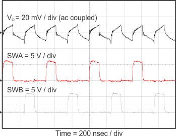 Figure 57. Full Load Output Voltage Ripple
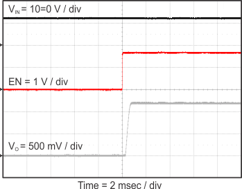 Figure 59. Start Up with EN
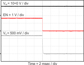 Figure 61. Shut Down with EN