ZHCSSP5D January 2009 – September 2023 TPS54332
PRODUCTION DATA
- 1
- 1 特性
- 2 应用
- 3 说明
- 4 Revision History
- 5 Pin Configuration and Functions
- 6 Specifications
-
7 Detailed Description
- 7.1 Overview
- 7.2 Functional Block Diagram
- 7.3
Feature Description
- 7.3.1 Fixed Frequency PWM Control
- 7.3.2 Voltage Reference (Vref)
- 7.3.3 Bootstrap Voltage (BOOT)
- 7.3.4 Enable and Adjustable Input Undervoltage Lockout (VIN UVLO)
- 7.3.5 Programmable Slow Start Using the SS Pin
- 7.3.6 Error Amplifier
- 7.3.7 Slope Compensation
- 7.3.8 Current Mode Compensation Design
- 7.3.9 Overcurrent Protection and Frequency Shift
- 7.3.10 Overvoltage Transient Protection
- 7.3.11 Thermal Shutdown
- 7.4 Device Functional Modes
-
8 Application and Implementation
- 8.1 Application Information
- 8.2
Typical Application
- 8.2.1 Design Requirements
- 8.2.2
Detailed Design Procedure
- 8.2.2.1 Custom Design with WEBENCH® Tools
- 8.2.2.2 Switching Frequency
- 8.2.2.3 Output Voltage Set Point
- 8.2.2.4 Input Capacitors
- 8.2.2.5 Output Filter Components
- 8.2.2.6 Inductor Selection
- 8.2.2.7 Capacitor Selection
- 8.2.2.8 Compensation Components
- 8.2.2.9 Bootstrap Capacitor
- 8.2.2.10 Catch Diode
- 8.2.2.11 Output Voltage Limitations
- 8.2.2.12 Power Dissipation Estimate
- 8.2.3 Application Curves
- 8.3 Power Supply Recommendations
- 8.4 Layout
- 9 Device and Documentation Support
- 10Mechanical, Packaging, and Orderable Information
7.3.4 Enable and Adjustable Input Undervoltage Lockout (VIN UVLO)
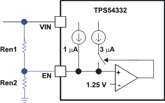
The EN pin has an internal pullup current source that provides the default condition of the TPS54332 operating when the EN pin floats.
The TPS54332 is disabled when the VIN pin voltage falls below internal VIN UVLO threshold. TI recommends using an external VIN UVLO to add Hysteresis unless VIN is greater than (VOUT + 2 V). To adjust the VIN UVLO with Hysteresis, use the external circuitry connected to the EN pin as shown in Figure 7-1. After the EN pin voltage exceeds 1.25 V, an additional 3 μA of hysteresis is added. Use Equation 1 and Equation 2 to calculate the resistor values needed for the desired VIN UVLO threshold voltages. The VSTART is the input start threshold voltage, the VSTOP is the input stop threshold voltage and the VEN is the enable threshold voltage of 1.25 V. The VSTOP must always be greater than 3.5 V.
