SLUS973A October 2009 – November 2016 TPS54290 , TPS54291 , TPS54292
PRODUCTION DATA.
- 1 Features
- 2 Applications
- 3 Description
- 4 Revision History
- 5 Device Comparison Table
- 6 Pin Configuration and Functions
- 7 Specifications
-
8 Detailed Description
- 8.1 Overview
- 8.2 Functional Block Diagram
- 8.3
Feature Description
- 8.3.1 Voltage Reference
- 8.3.2 Oscillator
- 8.3.3 Input UVLO and Start-Up
- 8.3.4 Enable and Timed Turnon of the Outputs
- 8.3.5 Soft Start
- 8.3.6 Output Voltage Regulation
- 8.3.7 Inductor Selection
- 8.3.8 Maximum Output Capacitance
- 8.3.9 Feedback Loop Compensation
- 8.3.10 Bootstrap for N-Channel MOSFET
- 8.3.11 Output Overload Protection
- 8.3.12 Operating Near Maximum Duty Cycle
- 8.3.13 Dual-Supply Operation
- 8.3.14 Bypassing and Filtering
- 8.4 Device Functional Modes
-
9 Application and Implementation
- 9.1 Application Information
- 9.2
Typical Applications
- 9.2.1
TPS54291 Design Example
- 9.2.1.1 Design Requirements
- 9.2.1.2
Detailed Design Procedure
- 9.2.1.2.1 Duty Cycle Estimation
- 9.2.1.2.2 Inductor Selection
- 9.2.1.2.3 Output Capacitor Selection
- 9.2.1.2.4 Input Capacitor Selection
- 9.2.1.2.5 Feedback
- 9.2.1.2.6 Compensation Components
- 9.2.1.2.7 Compensation Gain Setting Resistor
- 9.2.1.2.8 Compensation Integrator Capacitor
- 9.2.1.2.9 Bootstrap Capacitor
- 9.2.1.2.10 Power Dissipation
- 9.2.1.3 Application Curves
- 9.2.2 TPS54290 Cascaded Design Example
- 9.2.1
TPS54291 Design Example
- 10Power Supply Recommendations
- 11Layout
- 12Device and Documentation Support
- 13Mechanical, Packaging, and Orderable Information
9 Application and Implementation
NOTE
Information in the following applications sections is not part of the TI component specification, and TI does not warrant its accuracy or completeness. TI’s customers are responsible for determining suitability of components for their purposes. Customers should validate and test their design implementation to confirm system functionality.
9.1 Application Information
TPS5429X is a synchronous buck converter. It can convert an input voltage of 4.5 V to 18 V to two lower voltages. Channel 1 is rated for 1.5-A output, while Channel 2 is rated for 2.5-A output.
9.2 Typical Applications
9.2.1 TPS54291 Design Example
The following example illustrates the design process and component selection for a 12-V to 5-V or 3.3-V dual non-synchronous buck regulator using the TPS54291 converter.
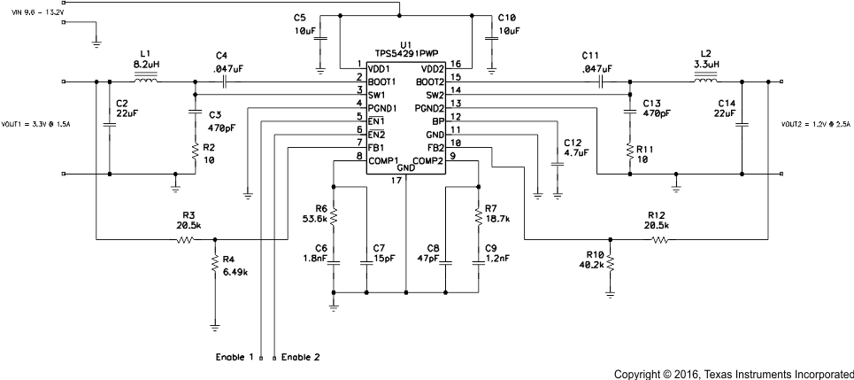 Figure 17. TPS54291 Design Example 1 Schematic
9.2.1.1 Design Requirements
A definition of symbols used can be found in Table 1. The efficiency, line regulation, and load regulation from printed-circuit boards built using this design are shown in Figure 19 and Figure 20.
Table 1. Design Example Electrical Characteristics
| PARAMETER | TEST CONDITIONS | MIN | TYP | MAX | UNIT | ||
|---|---|---|---|---|---|---|---|
| INPUT CHARACTERISTICS | |||||||
| VIN | Input voltage | 8 | 12 | 14 | V | ||
| IIN | Input current | VIN = nom, IOUT = max | A | ||||
| No load input current | VIN = nom, IOUT = 0 A | 12 | 20 | mA | |||
| VIN(UVLO) | Input UVLO | IOUT = min to max | 4 | 4.2 | 4.4 | V | |
| OUTPUT CHARACTERISTICS | |||||||
| VOUT1 | Output voltage 1 | VIN = nom, IOUT = nom | 3.2 | 3.3 | 3.4 | V | |
| VOUT2 | Output voltage 2 | VIN = nom, IOUT = nom | 1.15 | 1.2 | 1.25 | V | |
| Line regulation | VIN = min to max | 1% | |||||
| Load regulation | IOUT = min to max | 1% | |||||
| VOUT1(ripple) | Output1 voltage ripple | VIN = nom, IOUT1 = max | 50 | mVPP | |||
| VOUT2(ripple) | Output2 voltage ripple | VIN = nom, IOUT2 = max | 24 | mVPP | |||
| IOUT1 | Output current 1 | VIN = min to max | 0 | 1.5 | A | ||
| IOUT2 | Output current 2 | VIN = min to max | 0 | 2.5 | A | ||
| IOCP1 | Output overcurrent Channel 1 | VIN = nom, VOUT = (VOUT1 – 5%) | 1.8 | 2.2 | 2.6 | A | |
| IOCP2 | Output overcurrent Channel 2 | VIN = nom, VOUT = (VOUT2 – 5%) | 3.2 | 3.8 | 4.6 | A | |
| TRANSIENT RESPONSE | |||||||
| ΔVOUT | Change from load transient | ΔIOUT = 1 A at 3 µA/s | 200 | mV | |||
| Settling time | to 1% of VOUT | 1 | ms | ||||
| SYSTEMS CHARACTERISTICS | |||||||
| fSW | Switching frequency | 500 | 600 | 700 | kHz | ||
| ηPEAK | Peak efficiency | VIN = nom | 90% | ||||
| η | Full load efficiency | VIN = nom, IOUT = max | 80% | ||||
| TOP | Operating temperature | VIN = min to max, IOUT = min to max | 0 | 25 | 60 | °C | |
9.2.1.2 Detailed Design Procedure
The list of materials for this application is shown below in Table 2.
Table 2. Design Example List of Materials
| REFERENCE DESIGNATOR |
QTY | VALUE | DESCRIPTION | SIZE | PART NUMBER | MFR |
| C12 | 1 | 4.7 µF | Capacitor, Ceramic, 10 V, X5R, 20% | 0805 | Std | Std |
| C2, C14 | 2 | 22 µF | Capacitor, Ceramic, 6.3 V, X5R, 20% | 1206 | C3216X5R0J226M | TDK |
| C3, C13 | 2 | 470 pF | Capacitor, Ceramic, 25 V, X7R, 20% | 0603 | Std | Std |
| C4, C11 | 2 | 0.047 µF | Capacitor, Ceramic, 25 V, X7R, 20% | 0603 | Std | Std |
| C5, C10 | 2 | 10 µF | Capacitor, Ceramic, 25 V, X5R, 20% | 1210 | C3225X5R1E106M | TDK |
| C6 | 2 | 1.8 nF | Capacitor, Ceramic, 25 V, X7R, 20% | 0603 | Std | Std |
| C7 | 1 | 15 pF | Capacitor, Ceramic, 25 V, X7R, 20% | 0603 | Std | Std |
| C8 | 1 | 47 pF | Capacitor, Ceramic, 25 V, X7R, 20% | 0603 | Std | Std |
| C9 | 1 | 1.2 nF | Capacitor, Ceramic, 25 V, X7R, 20% | 0603 | Std | Std |
| L1 | 1 | 8.2 µH | Inductor, SMT, 4.38 A, 20 mΩ | 0.402 × 0.394 inch | MSS1048-822L | Coilcraft |
| L2 | 1 | 3.3 µH | Inductor, SMT, 5.04 A, 10 mΩ | 0.402 × 0.394 inch | MSS1048-332L | Coilcraft |
| R10 | 1 | 40.2 kΩ | Resistor, Chip, 1/16W, 1% | 0603 | Std | Std |
| R2, R11 | 2 | 10 Ω | Resistor, Chip, 1/16W, 5% | 0603 | Std | Std |
| R3, R12 | 2 | 20.5 kΩ | Resistor, Chip, 1/16W, 1% | 0603 | Std | Std |
| R4 | 1 | 6.49 kΩ | Resistor, Chip, 1/16W, 1% | 0603 | Std | Std |
| R6 | 1 | 7.87 kΩ | Resistor, Chip, 1/16W, 1% | 0603 | Std | Std |
| R7 | 1 | 4.64 kΩ | Resistor, Chip, 1/16W, 1% | 0603 | Std | Std |
| U1 | 1 | 2.5 A/1.5 A, 600 Hz | Dual Output Fully Synchronous Buck Converter w/Integrated FET | CSP | TPS54291PWP | TI |
9.2.1.2.1 Duty Cycle Estimation
The duty cycle of the main switching FET is estimated by Equation 12 and Equation 13.


9.2.1.2.2 Inductor Selection
The peak-to-peak ripple must be limited to between 20% and 30% of the maximum output current (see Equation 14 and Equation 15).


The minimum inductor size can be estimated by Equation 16 and Equation 17.


The standard inductor values of 8.2 µH and 3.3 µH are selected for Channel 1 and Channel 2, respectively. The actual ripple currents are estimated by Equation 18 and Equation 19.


The RMS current through the inductor is approximated by Equation 20 and Equation 21.


A DC current with 30% peak-to-peak ripple has an RMS current approximately 0.4% above the average current.
The peak inductor current is estimated by Equation 22 and Equation 23.


A 8.2-µH inductor with a minimum RMS current rating of 1.51 A and minimum saturation current rating of 3.7 A must be selected. A Coilcraft MSS1048-822ML 8.2-µH, 4.38-A inductor is chosen for Channel 1 and a Coilcraft MSS1048-332 3.3-µH inductor is chosen for Channel 2.
9.2.1.2.3 Output Capacitor Selection
Output capacitors are selected to support load transients and output ripple current. The minimum output capacitance to meet the transient specification is given by Equation 24 and Equation 25.


The maximum ESR to meet the ripple specification is given by Equation 26 and Equation 27.


A single 22-µF ceramic capacitor with approximately 2.5 mΩ of ESR is selected to provide sufficient margin for capacitance loss due to DC voltage bias.
9.2.1.2.4 Input Capacitor Selection
A minimum 10-µF ceramic input capacitor on each PVDD pin is recommended. The ceramic capacitor must handle the RMS ripple current in the input capacitor.
The RMS current in the input capacitors is estimated by Equation 28 and Equation 29.


One 1210 10-µF, 25-V, X5R, ceramic capacitor with 2-mΩ ESR and a 2-A RMS current rating are selected for each PVDD input. Higher voltage capacitors are selected to minimize capacitance loss at the DC bias voltage to ensure the capacitors have sufficient capacitance at the working voltage.
9.2.1.2.5 Feedback
The primary feedback divider resistor (RFB) from VOUT to FB must be selected between 10-kΩ and 100-kΩ to maintain a balance between power dissipation and noise sensitivity. For a 3.3-V and 5-V output, 20.5 kΩ is selected and the lower resistor is given by Equation 30.

For RFB = 20.5 kΩ and VFB = 0.8 V, RBIAS = 6.56 kΩ and 41.0 kΩ (6.49 kΩ and 40.2 kΩ selected) for 3.3 V and 1.2 V, respectively. It is common to select the next lower available resistor value for the bias resistor. This biases the nominal output voltage slightly higher, allowing additional tolerance for load regulation.
9.2.1.2.6 Compensation Components
The TPS54291 controller uses a transconductance error amplifier, which is compensated with a series capacitor and resistor to ground plus a high-frequency capacitor to reduce the gain at high frequency. To select the component, Equation 31 to Equation 33 define the control loop and power stage gain and transfer function.

where
- K = 5.6 × 10⁵ for TPS54290
- K = 1.5 × 10⁶ for TPS54291
- K = 3.6 × 10⁶ for TPS54292
The overall DC gain of the converter control-to-output transfer function is approximated by Equation 32.

With the power stage DC gain, it is possible to estimate the required mid-band gain to program a desired crossover frequency.

9.2.1.2.7 Compensation Gain Setting Resistor
RCOMP programs the mid-band error amplifier gain to set the desired crossover frequency in Equation 34.

9.2.1.2.8 Compensation Integrator Capacitor
An integrator capacitor provides maximum DC gain for the best possible DC regulation while programming the compensation zero to match the natural pole of the output filter (see Equation 35). CCOMP is selected by Equation 36.


9.2.1.2.9 Bootstrap Capacitor
To ensure proper charging of the high-side FET gate and limit the ripple voltage on the boost capacitor, a 47-nF boot strap capacitor is recommended.
9.2.1.2.10 Power Dissipation
The power dissipation in the TPS54291 is made from FET conduction losses, switching losses and regulator losses.
Conduction losses are estimated by Equation 37 and Equation 38.


The switching losses are estimated by Equation 39 and Equation 40.


The regulator losses are estimated by Equation 41.

Total power dissipation in the device is the sum of conduction losses and switching losses for both channels plus regulator losses, which is estimated to be 1.01 W.
9.2.1.3 Application Curves
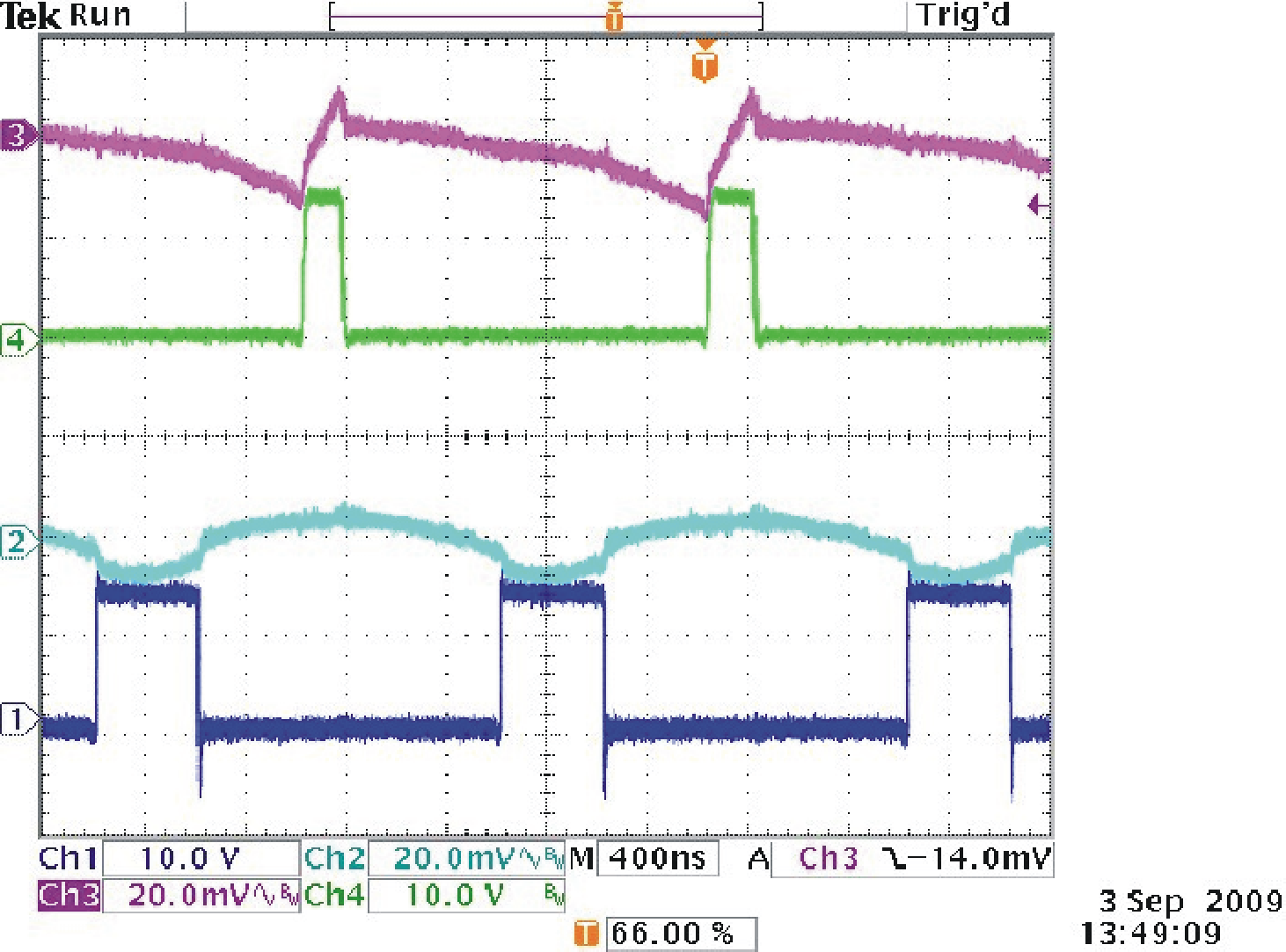 Figure 18. TPS54291 Design Example
Switching Waveforms
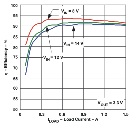 Figure 20. Design Efficiency for 3.3-V Output
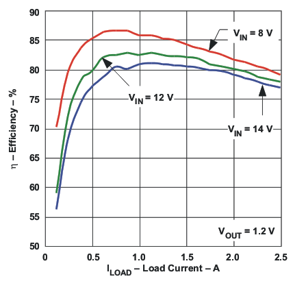 Figure 19. Design Efficiency for 1.2-V Output
9.2.2 TPS54290 Cascaded Design Example
TPS5429x can be configured as cascaded operation as shown in Figure 21. The 12-V input supply is applied to PVDD2 and the Channel 2 output is tied to PVDD1. The Channel 2 output is 3.3 V and capable of supporting 1.5 A to the load while generating power for the 1.2-V input for Channel 1.
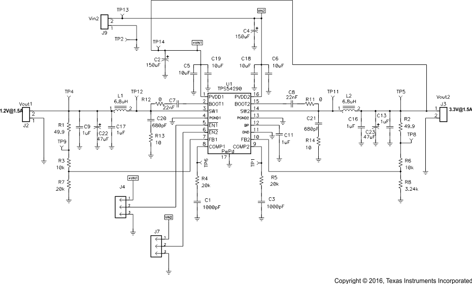 Figure 21. Cascading Operation
9.2.2.1 Application Curves
For Figure 22: Channel 1 is a 12-V supply, Channel 2 is VOUT1 (1.2 V), and Channel 3 is VOUT2(3.3 V).
For Figure 23: Channel 1 is Channel 1 SW node and Channel 2 is Channel 1 output ripple; Channel 3 is Channel 2 output ripple and Channel 2 is Channel 2 SW node.
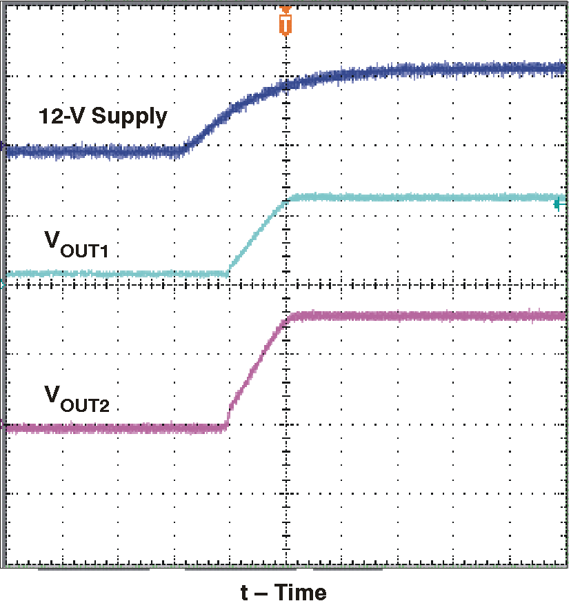 Figure 22. Start-Up Waveforms
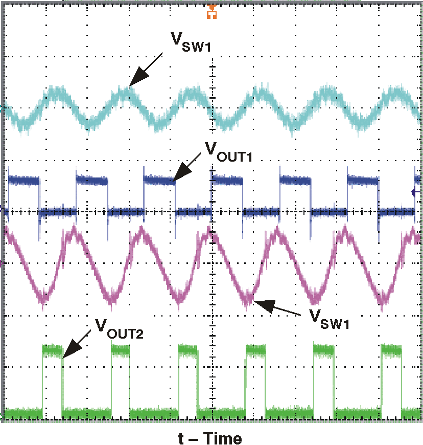 Figure 23. Output Ripple and SW Nodes