SLVS889C October 2008 – November 2014 TPS54140
PRODUCTION DATA.
- 1 Features
- 2 Applications
- 3 Description
- 4 Simplified Schematic
- 5 Revision History
- 6 Pin Configuration and Functions
- 7 Specifications
-
8 Detailed Description
- 8.1 Overview
- 8.2 Functional Block Diagram
- 8.3
Feature Description
- 8.3.1 Fixed Frequency PWM Control
- 8.3.2 Slope Compensation Output Current
- 8.3.3 Bootstrap Voltage (BOOT)
- 8.3.4 Low Dropout Operation
- 8.3.5 Error Amplifier
- 8.3.6 Voltage Reference
- 8.3.7 Adjusting the Output Voltage
- 8.3.8 Enable and Adjusting Undervoltage Lockout
- 8.3.9 Slow Start and Tracking Pin (SS/TR)
- 8.3.10 Overload-Recovery Circuit
- 8.3.11 Sequencing
- 8.3.12 Constant Switching Frequency and Timing Resistor (RT/CLK Pin)
- 8.3.13 Overcurrent Protection and Frequency Shift
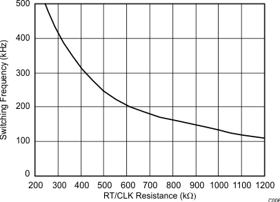
- 8.3.14 Selecting the Switching Frequency
- 8.3.15 How to Interface to RT/CLK Pin
- 8.3.16 Power Good (PWRGD Pin)
- 8.3.17 Overvoltage Transient Protection
- 8.3.18 Thermal Shutdown
- 8.3.19 Small-Signal Model for Loop Response
- 8.3.20 Simple Small-Signal Model for Peak-Current Mode Control
- 8.3.21 Small-Signal Model for Frequency Compensation
- 8.4 Device Functional Modes
-
9 Application and Implementation
- 9.1 Application Information
- 9.2
Typical Application
- 9.2.1 Design Requirements
- 9.2.2
Detailed Design Procedure
- 9.2.2.1 Selecting the Switching Frequency
- 9.2.2.2 Output Inductor Selection (LO)
- 9.2.2.3 Output Capacitor
- 9.2.2.4 Catch Diode
- 9.2.2.5 Input Capacitor
- 9.2.2.6 Slow-Start Capacitor
- 9.2.2.7 Bootstrap Capacitor Selection
- 9.2.2.8 Undervoltage-Lockout Set Point
- 9.2.2.9 Output Voltage and Feedback Resistors Selection
- 9.2.2.10 Compensation
- 9.2.2.11 Power Dissipation Estimate
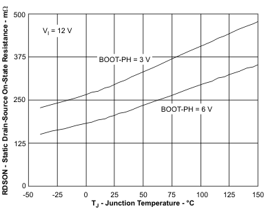
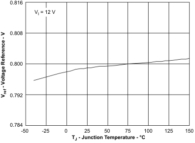
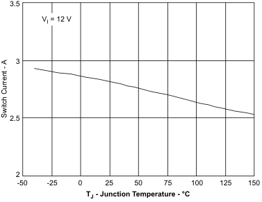
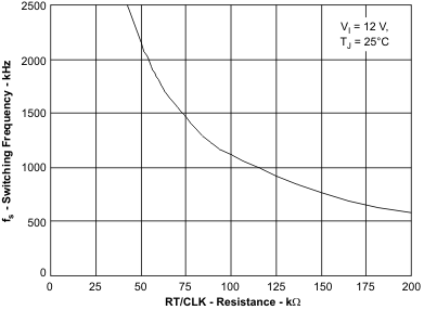
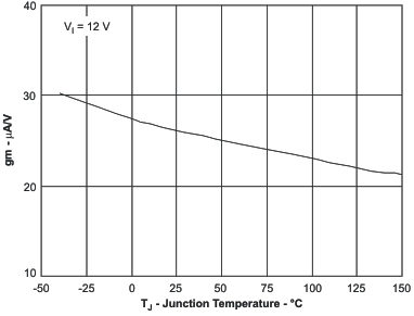
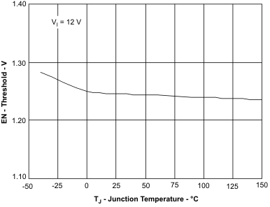
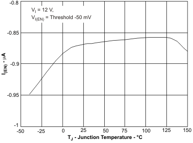
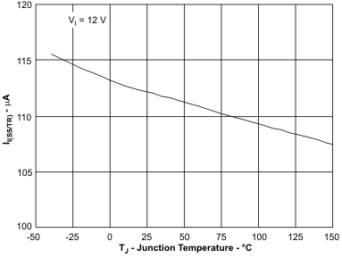
- 9.2.3 Application Curves
- 10Power Supply Recommendations
- 11Layout
- 12Device and Documentation Support
- 13Mechanical, Packaging, and Orderable Information
7 Specifications
7.1 Absolute Maximum Ratings(1)
Over operating temperature range (unless otherwise noted).| MIN | MAX | UNIT | ||
|---|---|---|---|---|
| Input voltage | VIN | –0.3 | 47 | V |
| EN | –0.3 | 5 | ||
| BOOT | 55 | |||
| VSENSE | –0.3 | 3 | ||
| COMP | –0.3 | 3 | ||
| PWRGD | –0.3 | 6 | ||
| SS/TR | –0.3 | 3 | ||
| RT/CLK | –0.3 | 3.6 | ||
| Output voltage | PH–BOOT | 8 | V | |
| PH | –0.6 | 47 | ||
| PH, 10-ns Transient | –2 | 47 | ||
| Voltage Difference | PAD to GND | ±200 | mV | |
| Source current | EN | 100 | μA | |
| BOOT | 100 | mA | ||
| VSENSE | 10 | μA | ||
| PH | Current Limit | A | ||
| RT/CLK | 100 | μA | ||
| Sink current | VIN | Current Limit | A | |
| COMP | 100 | μA | ||
| PWRGD | 10 | mA | ||
| SS/TR | 200 | μA | ||
| Operating junction temperature | –40 | 150 | °C | |
(1) Stresses beyond those listed under absolute maximum ratings may cause permanent damage to the device. These are stress ratings only and functional operation of the device at these or any other conditions beyond those indicated under recommended operating conditions is not implied. Exposure to absolute-maximum-rated conditions for extended periods may affect device reliability.
7.2 Handling Ratings
| MIN | MAX | UNIT | |||
|---|---|---|---|---|---|
| Tstg | Storage temperature range | –65 | 150 | °C | |
| V(ESD) | Electrostatic discharge | Human body model (HBM), per ANSI/ESDA/JEDEC JS-001, all pins(1) | –1 | 1 | kV |
| Charged device model (CDM), per JEDEC specification JESD22-C101, all pins(2) | –500 | 500 | V | ||
(1) JEDEC document JEP155 states that 500-V HBM allows safe manufacturing with a standard ESD control process.
(2) JEDEC document JEP157 states that 250-V CDM allows safe manufacturing with a standard ESD control process.
7.3 Recommended Operating Conditions
Over operating free-air temperature range (unless otherwise noted)| MIN | NOM | MAX | UNIT | ||
|---|---|---|---|---|---|
| Operating input voltage on the VIN pin | 3.5 | 42 | V | ||
| Output voltage | 0.8 | 39 | V | ||
| Output current | 0 | 1.5 | A | ||
| TJ | Operating junction temperature | –40 | 150 | °C | |
7.4 Thermal Information
| THERMAL METRIC(1) | DGQ | UNIT | |
|---|---|---|---|
| 10 PINS | |||
| RθJA | Junction-to-ambient thermal resistance | 67.4 | °C/W |
| RθJC(top) | Junction-to-case (top) thermal resistance | 46.7 | |
| RθJB | Junction-to-board thermal resistance | 38.4 | |
| ψJT | Junction-to-top characterization parameter | 1.9 | |
| ψJB | Junction-to-board characterization parameter | 38.4 | |
| RθJC(bot) | Junction-to-case (bottom) thermal resistance | 46.7 | |
(1) For more information about traditional and new thermal metrics, see the IC Package Thermal Metrics application report, SPRA953.
7.5 Electrical Characteristics
TJ = –40°C to 150°C, VIN = 3.5 to 42V (unless otherwise noted)7.6 Typical Characteristics