ZHCSCL8 July 2014 TPS54060-EP
PRODUCTION DATA.
- 1 特性
- 2 应用范围
- 3 说明
- 4 简化电路原理图
- 5 修订历史记录
- 6 Pin Configuration and Functions
- 7 Specifications
-
8 Detailed Description
- 8.1 Overview
- 8.2 Functional Block Diagram
- 8.3
Feature Description
- 8.3.1 Fixed Frequency PWM Control
- 8.3.2 Slope Compensation Output Current
- 8.3.3 Low-Dropout Operation and Bootstrap Voltage (Boot)
- 8.3.4 Error Amplifier
- 8.3.5 Voltage Reference
- 8.3.6 Adjusting the Output Voltage
- 8.3.7 Enable and Adjusting UVLO
- 8.3.8 Slow Start/Tracking Pin (SS/TR)
- 8.3.9 Overload Recovery Circuit
- 8.3.10 Sequencing
- 8.3.11 Constant Switching Frequency and Timing Resistor (RT/CLK Pin)
- 8.3.12 Overcurrent Protection and Frequency Shift
- 8.3.13 Selecting the Switching Frequency
- 8.3.14 How to Interface to RT/CLK Pin
- 8.3.15 Power Good (PWRGD Pin)
- 8.3.16 Overvoltage Transient Protection (OVTP)
- 8.3.17 Thermal Shutdown
- 8.3.18 Small Signal Model for Loop Response
- 8.3.19 Simple Small Signal Model for Peak Current Mode Control
- 8.3.20 Small Signal Model for Frequency Compensation
- 8.4 Device Functional Modes
-
9 Application and Implementation
- 9.1 Application Information
- 9.2
Typical Application
- 9.2.1 Design Requirements
- 9.2.2
Detailed Design Procedure
- 9.2.2.1 Selecting the Switching Frequency
- 9.2.2.2 Output Inductor Selection (LO)
- 9.2.2.3 Output Capacitor
- 9.2.2.4 Catch Diode
- 9.2.2.5 Input Capacitor
- 9.2.2.6 Slow Start Capacitor
- 9.2.2.7 Bootstrap Capacitor Selection
- 9.2.2.8 UVLO Set Point
- 9.2.2.9 Output Voltage and Feedback Resistors Selection
- 9.2.2.10 Compensation
- 9.2.3 Application Curves
- 10Power Supply Recommendations
- 11Layout
- 12器件和文档支持
- 13机械封装和可订购信息
9 Application and Implementation
9.1 Application Information
The TPS54060 device is a 60-V, 0.5-A, step-down regulator with an integrated high-side MOSFET.
9.2 Typical Application
9.2.1 Design Requirements
This example details the design of a high-frequency switching regulator using ceramic output capacitors. A few parameters must be known to start the design process. These parameters are typically determined at the system level. This example starts with the following known parameters:
Table 1. Design Parameters
| DESIGN PARAMETER | EXAMPLE VALUE |
|---|---|
| Output voltage | 3.3 V |
| Transient response 0- to 1.5-A load step | ΔVout = 4% |
| Maximum output current | 0.5 A |
| Input voltage | 34 V nominal 12 to 48 V |
| Output voltage ripple | 1% of Vout |
| Start input voltage (rising VIN) | 8.9 V |
| Stop input voltage (falling VIN) | 7.9 V |
9.2.2 Detailed Design Procedure
9.2.2.1 Selecting the Switching Frequency
The first step is to decide on a switching frequency for the regulator. Typically, the user should choose the highest switching frequency possible because this produces the smallest solution size. The high switching frequency allows for lower-valued inductors and smaller-output capacitors compared to a power supply that switches at a lower frequency. The switching frequency that the user can select is limited by the minimum on-time of the internal power switch, the input voltage, and the output voltage and the frequency shift limitation.
Equation 12 and Equation 13 must be used to find the maximum switching frequency for the regulator; choose the lower value of the two equations. Switching frequencies higher than these values result in pulse skipping or the lack of overcurrent protection during a short circuit.
The typical minimum on-time, tonmin, is 130 ns for the TPS54060. For this example, the output voltage is 3.3 V and the maximum input voltage is 48 V, which allows for a maximum switch frequency up to 616 kHz when including the inductor resistance, on-resistance, and diode voltage in Equation 12. To ensure overcurrent runaway is not a concern during short circuits in your design, use Equation 13 or the solid curve in Figure 40 to determine the maximum switching frequency. With a maximum input voltage of 48 V, assuming a diode voltage of 0.5 V, inductor resistance of 130 mΩ, switch resistance of 400 mΩ, a current limit value of 0.94 A, and a short-circuit output voltage of 0.1 V. The maximum switching frequency is approximately 923 kHz.
Choosing the lower of the two values and adding some margin, a switching frequency of 500 kHz is used. To determine the timing resistance for a given switching frequency, use Equation 11 or the curve in Figure 38.
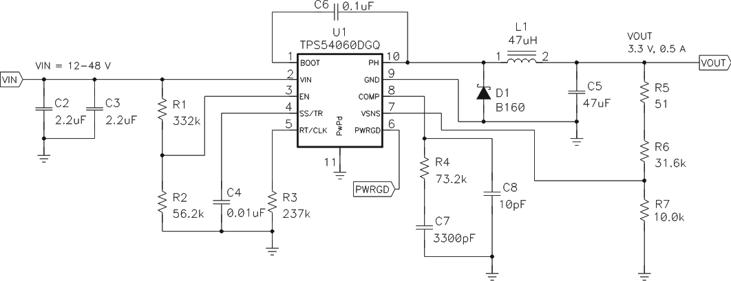
The switching frequency is set by resistor R3 shown in Figure 50.
Figure 50. High-Frequency, 3.3-V Output Power Supply Design With Adjusted UVLO
9.2.2.2 Output Inductor Selection (LO)
To calculate the minimum value of the output inductor, use Equation 28.
KIND is a coefficient that represents the amount of inductor ripple current relative to the maximum output current.
The inductor ripple current is filtered by the output capacitor. Therefore, choosing high inductor ripple currents impacts the selection of the output capacitor because the output capacitor must have a ripple current rating equal to or greater than the inductor ripple current. In general, the inductor ripple value is at the discretion of the designer; however, the following guidelines may be used.
For designs using low-ESR output capacitors such as ceramics, a value as high as KIND = 0.3 may be used. When using higher-ESR output capacitors, KIND = 0.2 yields better results. Because the inductor ripple current is part of the PWM control system, the inductor ripple current should always be greater than 30 mA for dependable operation. In a wide input voltage regulator, it is best to choose an inductor ripple current on the larger side. This allows the inductor to still have a measurable ripple current with the input voltage at its minimum.
For this design example, use KIND = 0.3, and the minimum inductor value is calculated to be 39.7 μH. For this design, a nearest standard value was chosen: 47 μH. For the output filter inductor, it is important that the RMS current and saturation current ratings not be exceeded. The RMS and peak inductor current can be found from Equation 30 and Equation 31.
For this design, the RMS inductor current is 0.501 A and the peak inductor current is 0.563 A. The chosen inductor is a MSS1048-473ML. It has a saturation current rating of 1.44 A and an RMS current rating of 1.83 A.
As the equation set demonstrates, lower ripple currents reduce the output voltage ripple of the regulator, but require a larger value of inductance. Selecting higher ripple currents increases the output voltage ripple of the regulator, but allows for a lower inductance value.
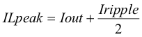
The current flowing through the inductor is the inductor ripple current plus the output current. During power up, faults or transient load conditions, the inductor current can increase above the calculated peak inductor current level calculated above. In transient conditions, the inductor current can increase up to the switch current limit of the device. For this reason, the most conservative approach is to specify an inductor with a saturation current rating equal to or greater than the switch current limit rather than the peak inductor current.
9.2.2.3 Output Capacitor
To select the value of the output capacitor, account for three primary considerations. The output capacitor determines the modulator pole, the output voltage ripple, and how the regulators respond to a large change in load current. The output capacitance must be selected based on the most stringent of these three criteria.
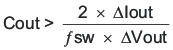
The first criterion is the desired response to a large change in the load current. The output capacitor needs to supply the load with current when the regulator cannot. This situation would occur if there are desired hold-up times for the regulator where the output capacitor must hold the output voltage above a certain level for a specified amount of time after the input power is removed. Also, the regulator will temporarily not be able to supply sufficient output current if there is a large, fast increase in the current needs of the load such as transitioning from no load to a full load. The regulator usually needs two or more clock cycles for the control loop to see the change in load current and output voltage and adjust the duty cycle to react to the change. The output capacitor must be sized to supply the extra current to the load until the control loop responds to the load change. The output capacitance must be large enough to supply the difference in current for 2 clock cycles while only allowing a tolerable amount of droop in the output voltage. Equation 32 shows the minimum output capacitance necessary to accomplish this.
Where ΔIout is the change in output current, ƒsw is the regulators switching frequency and ΔVout is the allowable change in the output voltage. For this example, the transient load response is specified as a 4% change in Vout for a load step from 0 A (no load) to 0.5 A (full load). For this example, ΔIout = 0.5 – 0 = 0.5 A and ΔVout = 0.04 × 3.3 = 0.132 V. Using these numbers gives a minimum capacitance of 15.2 μF. This value does not take the ESR of the output capacitor into account in the output voltage change. For ceramic capacitors, the ESR is usually small enough to ignore in this calculation. Aluminum electrolytic and tantalum capacitors have higher ESR that should be taken into account.
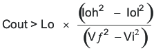
The catch diode of the regulator cannot sink current, so any stored energy in the inductor will produce an output voltage overshoot when the load current rapidly decreases (see Figure 51). The output capacitor must also be sized to absorb energy stored in the inductor when transitioning from a high load current to a lower load current. The excess energy that gets stored in the output capacitor increases the voltage on the capacitor. The capacitor must be sized to maintain the desired output voltage during these transient periods. Equation 33 is used to calculate the minimum capacitance to keep the output voltage overshoot to a desired value. Where L is the value of the inductor, IOH is the output current under heavy load, IOL is the output under light load, VF is the final peak output voltage, and Vi is the initial capacitor voltage. For this example, the worst case load step is from 0.5 A to 0 A. The output voltage increases during this load transition and the stated maximum in our specification is 4% of the output voltage. This makes Vf = 1.04 × 3.3 = 3.432. Vi is the initial capacitor voltage, which is the nominal output voltage of 3.3 V. Using these numbers in Equation 33 yields a minimum capacitance of 13.2 μF.
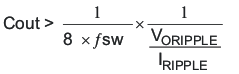
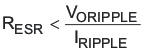
Equation 34 calculates the minimum output capacitance needed to meet the output voltage ripple specification. Where ƒsw is the switching frequency, Voripple is the maximum allowable output voltage ripple, and Iripple is the inductor ripple current. Equation 34 yields 1 μF.
Equation 35 calculates the maximum ESR an output capacitor can have to meet the output voltage ripple specification. Equation 35 indicates the ESR should be less than 248 mΩ.
The most stringent criterion for the output capacitor is 15.2 μF of capacitance to keep the output voltage in regulation during a load transient.
Additional capacitance deratings for aging, temperature, and DC bias should be factored in which will increase this minimum value. For this example, a 47-μF 10-V X5R ceramic capacitor with 5 mΩ of ESR is used.
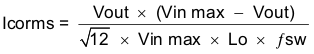
Capacitors generally have limits to the amount of ripple current they can handle without failing or producing excess heat. An output capacitor that can support the inductor ripple current must be specified. Some capacitor data sheets specify the root mean square (RMS) value of the maximum ripple current. Equation 36 can be used to calculate the RMS ripple current the output capacitor needs to support. For this application, Equation 36 yields 37.7 mA.
9.2.2.4 Catch Diode
The TPS54060 requires an external catch diode between the PH pin and GND. The selected diode must have a reverse voltage rating equal to or greater than Vinmax. The peak current rating of the diode must be greater than the maximum inductor current. The diode should also have a low forward voltage. Schottky diodes are typically a good choice for the catch diode due to their low forward voltage. The lower the forward voltage of the diode, the higher the efficiency of the regulator.
Typically, the higher the voltage and current ratings the diode has, the higher the forward voltage is. Because the design example has an input voltage up to 48 V, a diode with a minimum of 60-V reverse voltage is selected.
For the example design, the B160A Schottky diode is selected for its lower forward voltage and it comes in a larger package size which has good thermal characteristics over small devices. The typical forward voltage of the B160A is 0.5 V.
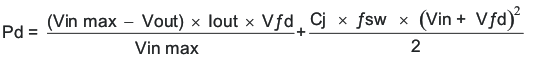
The diode must be selected with an appropriate power rating. The diode conducts the output current during the off-time of the internal power switch. The off-time of the internal switch is a function of the maximum input voltage, output voltage, and switching frequency. The output current during the off-time is multiplied by the forward voltage of the diode which equals the conduction losses of the diode. At higher switch frequencies, the AC losses of the diode need to be taken into account. The AC losses of the diode are due to the charging and discharging of the junction capacitance and reverse recovery. Equation 37 is used to calculate the total power dissipation, conduction losses plus AC losses, of the diode.
The B160A has a junction capacitance of 110 pF. Using Equation 37, the selected diode will dissipate 0.297 W. This power dissipation, depending on mounting techniques, should produce a 5.9°C temperature rise in the diode when the input voltage is 48 V and the load current is 0.5 A.
If the power supply spends a significant amount of time at light load currents or in sleep mode, consider using a diode which has a low leakage current and slightly higher forward voltage drop.
9.2.2.5 Input Capacitor
The TPS54060 requires a high-quality ceramic, type X5R or X7R, input decoupling capacitor of at least 3 μF of effective capacitance, and in some applications, a bulk capacitance. The effective capacitance includes any DC bias effects. The voltage rating of the input capacitor must be greater than the maximum input voltage. The capacitor must also have a ripple current rating greater than the maximum input current ripple of the TPS54060. The input ripple current can be calculated using Equation 38.
The value of a ceramic capacitor varies significantly over temperature and the amount of DC bias applied to the capacitor. The capacitance variations due to temperature can be minimized by selecting a dielectric material that is stable over temperature. X5R and X7R ceramic dielectrics are usually selected for power regulator capacitors because they have a high capacitance to volume ratio and are fairly stable over temperature. The output capacitor must also be selected with the DC bias taken into account. The capacitance value of a capacitor decreases as the DC bias across a capacitor increases.
For this example design, a ceramic capacitor with at least a 60-V voltage rating is required to support the maximum input voltage. Common standard ceramic capacitor voltage ratings include 4 V, 6.3 V, 10 V, 16 V, 25 V, 50 V, or 100 V, so a 100-V capacitor should be selected. For this example, two 2.2-μF, 100-V capacitors in parallel are selected. Table 2 shows a selection of high-voltage capacitors. The input capacitance value determines the input ripple voltage of the regulator. The input voltage ripple can be calculated using Equation 39. Using the design example values, Ioutmax = 0.5 A, Cin = 4.4 μF, ƒsw = 500 kHz, yields an input voltage ripple of 57 mV and a rms input ripple current of 0.223 A.
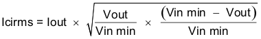
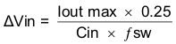
Table 2. Capacitor Types
| VENDOR | VALUE (μF) | EIA SIZE | VOLTAGE | DIELECTRIC | COMMENTS |
|---|---|---|---|---|---|
| Murata | 1.0 to 2.2 | 1210 | 100 V | X7R | GRM32 series |
| 1.0 to 4.7 | 50 V | ||||
| 1.0 | 1206 | 100 V | GRM31 series | ||
| 1.0 to 2.2 | 50 V | ||||
| Vishay | 1.0 10 1.8 | 2220 | 50 V | VJ X7R series | |
| 1.0 to 1.2 | 100 V | ||||
| 1.0 to 3.9 | 2225 | 50 V | |||
| 1.0 to 1.8 | 100 V | ||||
| TDK | 1.0 to 2.2 | 1812 | 100 V | C series C4532 | |
| 1.5 to 6.8 | 50 V | ||||
| 1.0. to 2.2 | 1210 | 100 V | C series C3225 | ||
| 1.0 to 3.3 | 50 V | ||||
| AVX | 1.0 to 4.7 | 1210 | 50 V | X7R dielectric series | |
| 1.0 | 100 V | ||||
| 1.0 to 4.7 | 1812 | 50 V | |||
| 1.0 to 2.2 | 100 V |
9.2.2.6 Slow Start Capacitor
The slow start capacitor determines the minimum amount of time it takes for the output voltage to reach its nominal programmed value during power up. This is useful if a load requires a controlled voltage slew rate. This is also used if the output capacitance is large and would require large amounts of current to quickly charge the capacitor to the output voltage level. The large currents necessary to charge the capacitor may make the TPS54060 reach the current limit or excessive current draw from the input power supply may cause the input voltage rail to sag. Limiting the output voltage slew rate solves both of these problems.
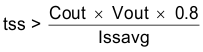
The slow start time must be long enough to allow the regulator to charge the output capacitor up to the output voltage without drawing excessive current. Equation 40 can be used to find the minimum slow start time, tss, necessary to charge the output capacitor, Cout, from 10% to 90% of the output voltage, Vout, with an average slow start current of Issavg. In the example, to charge the 47-μF output capacitor up to 3.3 V while only allowing the average input current to be 0.125 A would require a 1-ms slow start time.
After the slow start time is known, the slow start capacitor value can be calculated using Equation 6. For the example circuit, the slow start time is not too critical because the output capacitor value is 47 μF which does not require much current to charge to 3.3 V. The example circuit has the slow start time set to an arbitrary value of 3.2 ms, which requires a 0.01-μF capacitor.
9.2.2.7 Bootstrap Capacitor Selection
A 0.1-μF ceramic capacitor must be connected between the BOOT and PH pins for proper operation. TI recommends to use a ceramic capacitor with X5R or better grade dielectric. The capacitor should have a 10 V or higher voltage rating.
9.2.2.8 UVLO Set Point
The UVLO can be adjusted using an external voltage divider on the EN pin of the TPS54060. The UVLO has two thresholds, one for power up when the input voltage is rising and one for power down or brown outs when the input voltage is falling. For the example design, the supply should turn on and start switching after the input voltage increases above 8.9 V (enabled). After the regulator starts switching, it should continue to do so until the input voltage falls below 7.9 V (UVLO stop).
The programmable UVLO and enable voltages are set using a resistor divider between Vin and ground to the EN pin. Equation 2 through Equation 3 can be used to calculate the resistance values necessary. For the example application, a 332-kΩ resistor between Vin and EN and a 56.2-kΩ resistor between EN and ground are required to produce the 8.9- and 7.9-V start and stop voltages.
9.2.2.9 Output Voltage and Feedback Resistors Selection
For the example design, 10 kΩ was selected for R2. Using Equation 1, R1 is calculated as 31.25 kΩ. The nearest standard 1% resistor is 31.6 kΩ. Due to current leakage of the VSENSE pin, the current flowing through the feedback network should be greater than 1 μA to maintain the output voltage accuracy. This requirement makes the maximum value of R2 equal to 800 kΩ. Using higher resistor values decreases quiescent current and improves efficiency at low output currents, but may introduce noise immunity problems.
9.2.2.10 Compensation
There are several methods used to compensate DC/DC regulators. The method presented here is easy to calculate and ignores the effects of the slope compensation that is internal to the device. Because the slope compensation is ignored, the actual crossover frequency is usually lower than the crossover frequency used in the calculations. This method assumes the crossover frequency is between the modulator pole and the ESR zero and the ESR zero is at least 10 times greater the modulator pole. Use SwitcherPro software for a more accurate design.
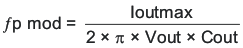
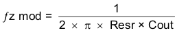
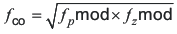
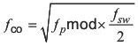
To get started, the modulator pole, ƒpmod, and the ESR zero, ƒz1 must be calculated using Equation 41 and Equation 42. For Cout, use a derated value of 40 μf. Use equations Equation 43 and Equation 44, to estimate a starting point for the crossover frequency, ƒco, to design the compensation. For the example design, ƒpmod is 603 Hz and ƒzmod is 796 kHz. Equation 43 is the geometric mean of the modulator pole and the ESR zero, and Equation 44 is the mean of modulator pole and the switching frequency. Equation 43 yields 21.9 kHz and Equation 44 gives 12.3 kHz. Use the lower value of Equation 43 or Equation 44 for an initial crossover frequency. For this example, ƒco is 12.3 kHz. Next, the compensation components are calculated. A resistor in series with a capacitor is used to create a compensating zero. A capacitor in parallel to these two components forms the compensating pole.
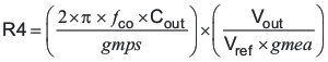
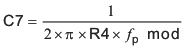
To determine the compensation resistor, R4, use Equation 45. Assume the power stage transconductance, gmps, is 1.9 A/V. The output voltage, Vo, reference voltage, VREF, and amplifier transconductance, gmea, are 3.3 V, 0.8 V, and 92 μA/V, respectively. R4 is calculated to be 72.6 kΩ, use the nearest standard value of 73.2 kΩ. Use Equation 46 to set the compensation zero to the modulator pole frequency. Equation 46 yields 3600 pF for compensating capacitor C7, a 3300 pF is used on the board.
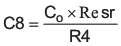
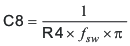
Use the larger value of Equation 47 and Equation 48 to calculate the C8, to set the compensation pole. Equation 48 yields 8.7 pF so the nearest standard of 10 pF is used.
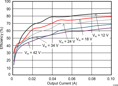
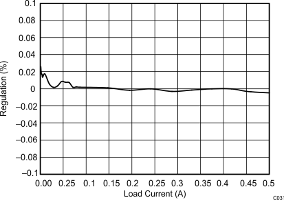
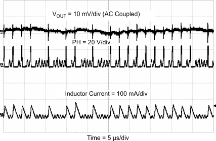
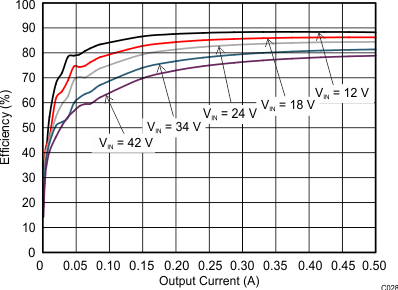
9.2.3 Application Curves
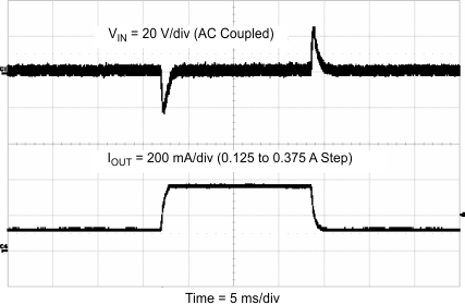
| Time = 5 ms/div | ||
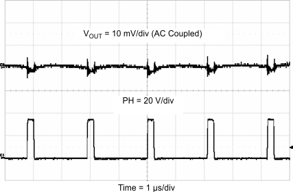
| Time = 1 µs/div | ||
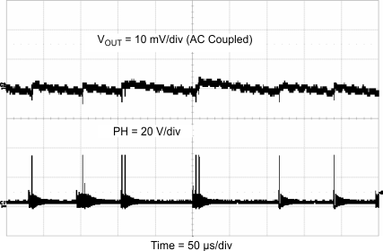
| Time = 50 µs/div | ||
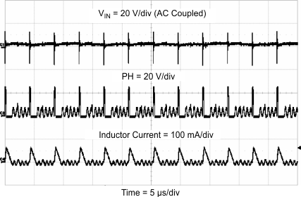
| Time = 5 µs/div | ||
| VOUT = 3.3 V | ||
| VI = 34 V | ||
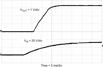
| Time = 2 ms/div | ||
| Time = 5 µs/div | ||
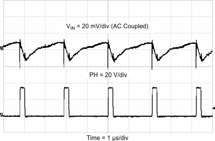
| Time = 1 µs/div | ||
| VOUT = 3.3 V | ||
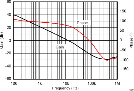
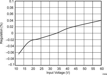
| IO = 0.25 A | ||