ZHCS453D August 2011 – April 2021 TPS53353
PRODUCTION DATA
- 1 特性
- 2 应用
- 3 说明
- 4 Revision History
- 5 Pin Configuration and Functions
- 6 Specifications
-
7 Detailed Description
- 7.1 Overview
- 7.2 Functional Block Diagram
- 7.3
Feature Description
- 7.3.1 5-V LDO and VREG Start-Up
- 7.3.2 Adaptive On-Time D-CAP™ Control and Frequency Selection
- 7.3.3 Ramp Signal
- 7.3.4 Adaptive Zero Crossing
- 7.3.5 Power-Good
- 7.3.6 Current Sense, Overcurrent and Short Circuit Protection
- 7.3.7 Overvoltage and Undervoltage Protection
- 7.3.8 UVLO Protection
- 7.3.9 Thermal Shutdown
- 7.4 Device Functional Modes
- 8 Application and Implementation
- 9 Power Supply Recommendations
- 10Layout
- 11Device and Documentation Support
6.6 Typical Characteristics
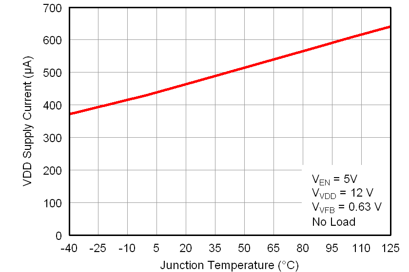 Figure 6-1 VDD Supply Current vs. Junction Temperature
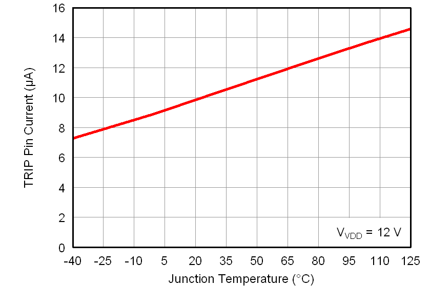 Figure 6-3 TRIP Pin Current vs. Junction Temperature
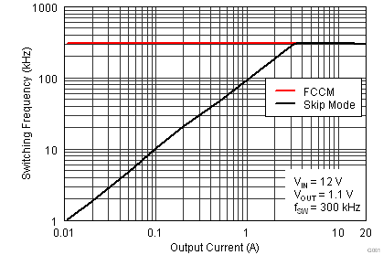 Figure 6-5 Switching Frequency vs. Output Current
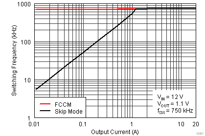 Figure 6-7 Switching Frequency vs. Output Current
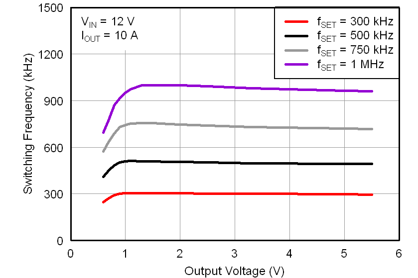 Figure 6-9 Switching Frequency vs. Output Voltage
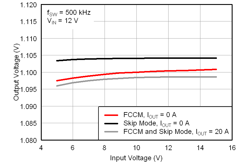 Figure 6-11 Output Voltage vs. Input Voltage
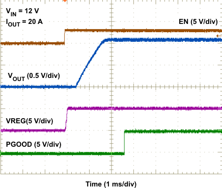 Figure 6-13 Start-Up Waveforms
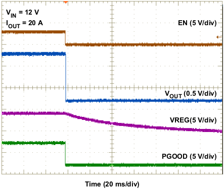 Figure 6-15 Shutdown Waveforms
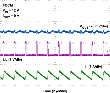 Figure 6-17 1.1-V Output FCCM Mode Steady-State Operation
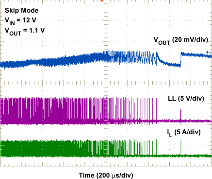 Figure 6-19 CCM-to-DCM Transition Waveforms
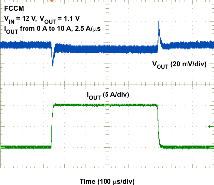 Figure 6-21 FCCM Load Transient
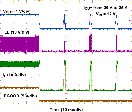 Figure 6-23 Overcurrent Protection Waveforms
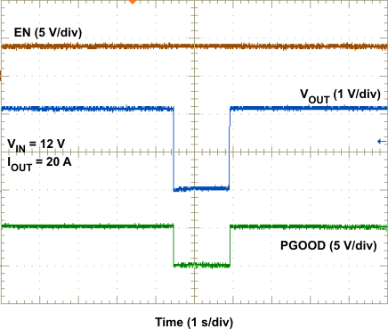 Figure 6-25 Overtemperature Protection Waveforms
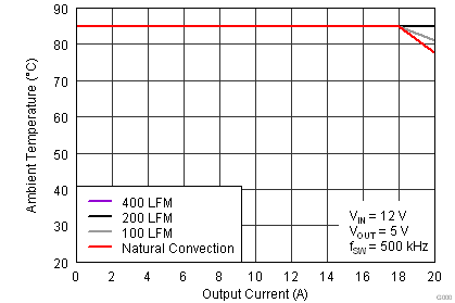 Figure 6-27 Safe Operating Area
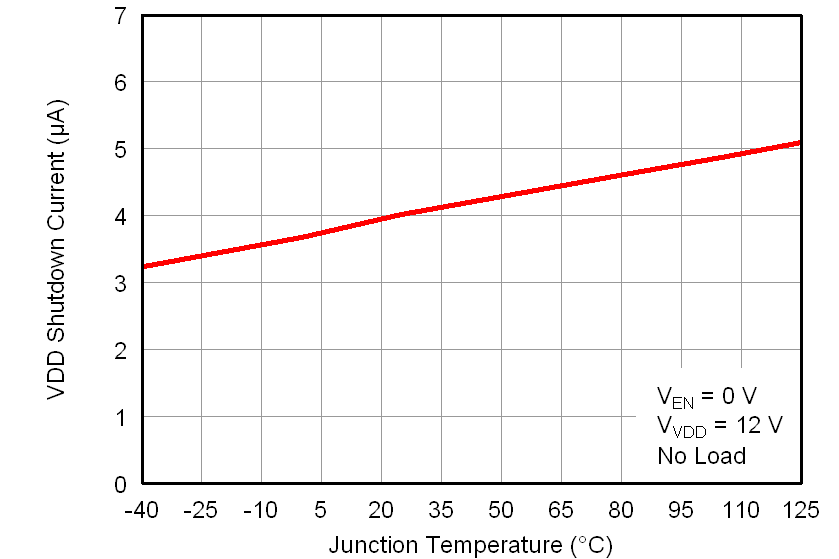 Figure 6-2 VDD Shutdown Current vs. Junction Temperature
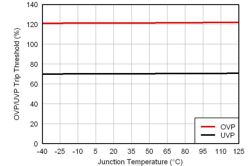 Figure 6-4 OVP/UVP Trip Threshold vs. Junction Temperature
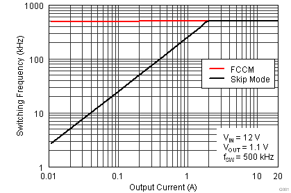 Figure 6-6 Switching Frequency vs. Output Current
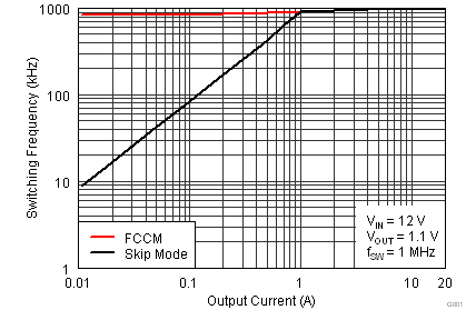 Figure 6-8 Switching Frequency vs. Output Current
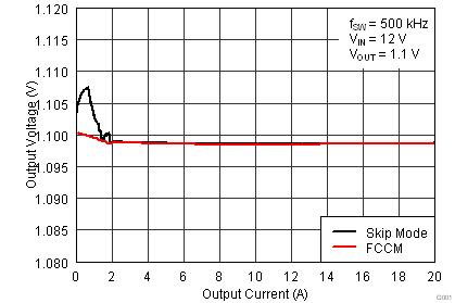 Figure 6-10 Output Voltage vs. Output Current
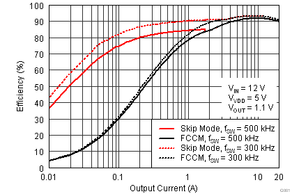 Figure 6-12 Efficiency vs Output Current
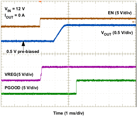 Figure 6-14 Prebias Start-Up Waveforms
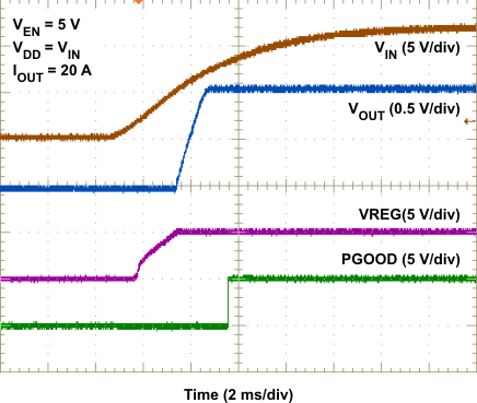 Figure 6-16 UVLO Start-Up Waveforms
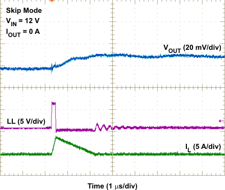 Figure 6-18 1.1-V Output Skip Mode Steady-State Operation
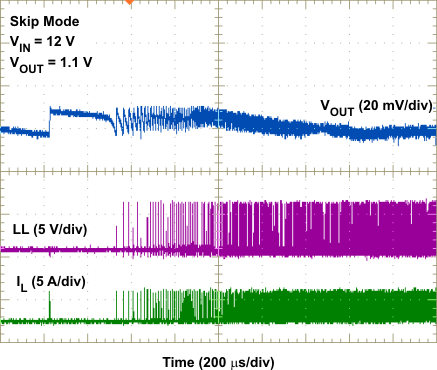 Figure 6-20 DCM-to-CCM Transition Waveforms
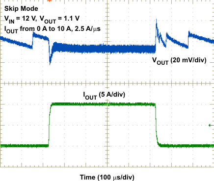 Figure 6-22 Skip Mode Load Transeint
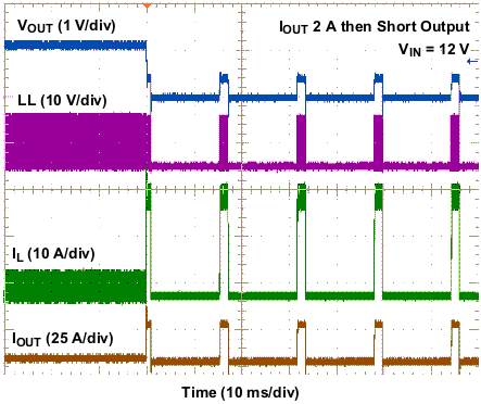 Figure 6-24 Output Short-Circuit Protection Waveforms
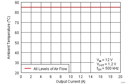 Figure 6-26 Safe Operating Area
For VOUT = 5 V, an SC5026-1R0 inductor is used. For 1 ≤ VOUT ≤ 3.3 V, a PA0513.441 inductor is used
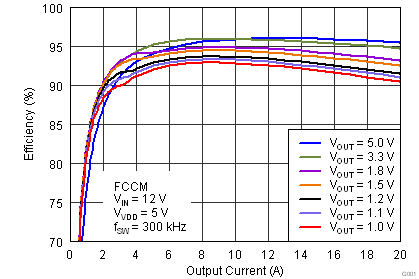 Figure 6-28 Efficiency vs Output Current
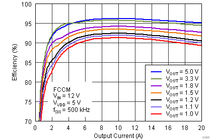 Figure 6-30 Efficiency vs Output Current
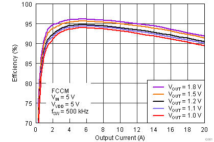 Figure 6-32 Efficiency vs Output Current
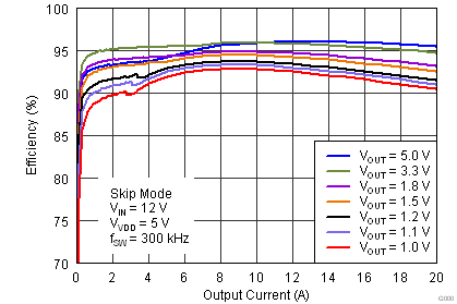 Figure 6-29 Efficiency vs Output Current
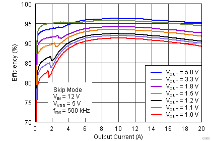 Figure 6-31 Efficiency vs Output Current
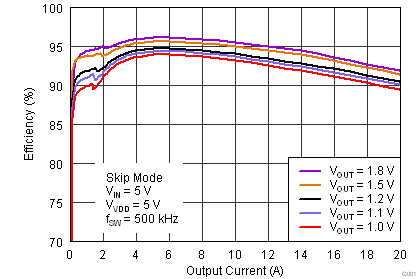 Figure 6-33 Efficiency vs Output Current