SLUS909B May 2009 – August 2014 TPS53126
PRODUCTION DATA.
- 1 Features
- 2 Applications
- 3 Description
- 4 Simplified Schematics
- 5 Revision History
- 6 Pin Configurations and Functions
- 7 Specifications
-
8 Detailed Description
- 8.1 Overview
- 8.2 Functional Block Diagram
- 8.3
Feature Description
- 8.3.1 PWM Operation
- 8.3.2 Drivers
- 8.3.3 PWM Frequency And Adaptive On-time Control
- 8.3.4 5 Volt Regulator
- 8.3.5 Soft Start
- 8.3.6 Pre-Bias Support
- 8.3.7 Switching Frequency Selection
- 8.3.8 Output Discharge Control
- 8.3.9 Overcurrent Limit
- 8.3.10 Over/under Voltage Protection
- 8.3.11 UVLO Protection
- 8.3.12 Thermal Shutdown
- 8.4 Device Functional Modes
- 9 Application and Implementation
- 10Power Supply Recommendations
- 11Layout
- 12Device and Documentation Support
- 13Mechanical, Packaging, and Orderable Information
封装选项
请参考 PDF 数据表获取器件具体的封装图。
机械数据 (封装 | 引脚)
- RGE|24
- PW|24
散热焊盘机械数据 (封装 | 引脚)
- RGE|24
订购信息
7 Specifications
7.1 Absolute Maximum Ratings
over operating free-air temperature range (unless otherwise noted) (1)| MIN | MAX | UNIT | |||
|---|---|---|---|---|---|
| Input voltage | VIN, EN1, EN2 | –0.3 | 26 | V | |
| VBST1, VBST2 | –0.3 | 32 | |||
| VBST1, VBST2 (wrt SWx) | –0.3 | 6 | |||
| V5FILT, VFB1, VFB2, TRIP1, TRIP2, VO1, VO2, TEST1, TEST2 | –0.3 | 6 | |||
| SW1, SW2 | –2 | 26 | |||
| Output voltage | DRVH1, DRVH2 | –1 | 32 | V | |
| DRVH1, DRVH2 (wrt SWx) | –0.3 | 6 | |||
| DRVL1, DRVL2, VREG5 | –0.3 | 6 | |||
| PGND1, PGND2 | –0.3 | 0.3 | |||
| TA | Operating ambient temperature range | –40 | 85 | °C | |
| TJ | Junction temperature range | –40 | 150 | °C | |
(1) Stresses beyond those listed under Absolute Maximum Ratings may cause permanent damage to the device. These are stress ratings only, which do not imply functional operation of the device at these or any other conditions beyond those indicated under Recommended Operating Conditions. Exposure to absolute-maximum-rated conditions for extended periods may affect device reliability.
7.2 Handling Ratings
| MIN | MAX | UNIT | |||
|---|---|---|---|---|---|
| Tstg | Storage temperature range | –55 | 150 | °C | |
| V(ESD) | Electrostatic discharge | Human body model (HBM), per ANSI/ESDA/JEDEC JS-001, all pins(1) | –2000 | 2000 | V |
| Charged device model (CDM), per JEDEC specification JESD22-C101, all pins(2) | –500 | 500 | |||
(1) JEDEC document JEP155 states that 500-V HBM allows safe manufacturing with a standard ESD control process.
(2) JEDEC document JEP157 states that 250-V CDM allows safe manufacturing with a standard ESD control process.
7.3 Recommended Operating Conditions
| MIN | MAX | UNIT | |||
|---|---|---|---|---|---|
| Supply input voltage range | VIN | 4.5 | 24 | V | |
| V5FILT | 4.5 | 5.5 | |||
| Input voltage range | VBST1, VBST2 | –0.1 | 30 | V | |
| VBST1, VBST2 (wrt SWx) | –0.1 | 5.5 | |||
| VFB1, VFB2, VO1, VO2, TEST1, TEST2 | –0.1 | 5.5 | |||
| TRIP1, TRIP2 | –0.1 | 0.3 | |||
| EN1, EN2 | –0.1 | 24 | |||
| SW1, SW2 | –1.8 | 24 | |||
| Output voltage range | DRVH1, DRVH2 | –0.1 | 30 | V | |
| VBST1, VBST2 (wrt SWx) | –0.1 | 5.5 | |||
| DRVL1, DRVL2, VREG5 | –0.1 | 5.5 | |||
| PGND1, PGND2 | –0.1 | 0.1 | |||
| TA | Operating free-air temperature | –40 | 85 | °C | |
| TJ | Operating junction temperature | –40 | 125 | °C | |
7.4 Thermal Information
| THERMAL METRIC(1) | TPS53126 | UNIT | ||
|---|---|---|---|---|
| PW (24 PINS) | RGE( 24 PINS) | |||
| RθJA | Junction-to-ambient thermal resistance | 88.9 | 35.4 | °C/W |
| RθJC(top) | Junction-to-case (top) thermal resistance | 26.5 | 39.1 | |
| RθJB | Junction-to-board thermal resistance | 43.5 | 13.6 | |
| ψJT | Junction-to-top characterization parameter | 1.1 | 0.5 | |
| ψJB | Junction-to-board characterization parameter | 43.0 | 13.6 | |
| RθJC(bot) | Junction-to-case (bottom) thermal resistance | n/a | 3.8 | |
(1) For more information about traditional and new thermal metrics, see the IC Package Thermal Metrics application report, SPRA953.
7.5 Electrical Characteristics
over recommended free-air temperature range, VIN = 12 V (Unless otherwise noted)| PARAMETER | TEST CONDITIONS | MIN | TYP | MAX | UNIT | |
|---|---|---|---|---|---|---|
| SUPPLY CURRENT | ||||||
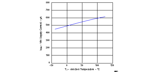
| IIN | VIN supply current | VIN current, TA = 25°C, VREG5 tied to V5FLT, EN1 = EN2 = 5V, VFB1 = VFB2 = 0.8V, SW1 = SW2 = 0.5V | 450 | 800 | μA | |
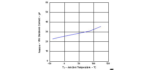
| IVINSDN | VIN shutdown current | VIN current, TA = 25°C, No load, EN1 = EN2 = 0 V, VREG5 = ON | 30 | 60 | μA | |
| VFB VOLTAGE and DISCHARGE RESISTANCE | ||||||
| VBG | Bandgap initial regulation accuracy | TA = 25°C | -1.0% | 1.0% | ||
| VVFBTHLx | VFBx threshold voltage | TA = 25°C, TEST2 = 0 V, SWinj = OFF | 755 | 765 | 775 | mV |
| TA = –40°C to 85°C, TEST2 = 0 V, SWinj = OFF(1) | 752 | 778 | ||||
| VVFBTHHx | VFBx threshold voltage | TA = 25°C, TEST2 = V5FILT, SWinj = OFF | 748 | 758 | 768 | mV |
| TA = –40°C to 85°C, TEST2 = V5FILT, SWinj = OFF(1) | 745 | 771 | ||||
| IVFB | VFB input current | VFBx = 0.8 V, TA = 25°C | –0.01 | ±0.1 | μA | |
| RDischg | VO discharge resistance | ENx = 0 V, VOx = 0.5 V, TA = 25°C | 40 | 80 | Ω | |
| VREG5 OUTPUT | ||||||
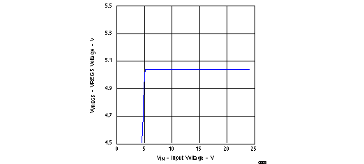
| VVREG5 | VREG5 output voltage | TA = 25°C, 5.5 V < VIN < 24 V, 0 < IVREG5 < 10 mA |
4.6 | 5.0 | 5.2 | V |
| VLN5 | Line regulation | 5.5 V < VIN < 24 V, IVREG5 = 10 mA | 20 | mV | ||
| VLD5 | Load regulation | 1 mA < IVREG5 < 10 mA | 40 | mV | ||
| IVREG5 | Output current | VIN = 5.5 V, VVREG5 = 4 V, TA = 25°C | 170 | mA | ||
| OUTPUT: N-CHANNEL MOSFET GATE DRIVERS | ||||||
| RDRVH | DRVH resistance | Source, IDRVHx = –100 mA | 5.5 | 11 | Ω | |
| Sink, IDRVHx = 100 mA | 2.5 | 5 | ||||
| RDRVL | DRVL resistance | Source, IDRVLx = –100 mA | 4 | 12 | Ω | |
| Sink, IDRVLx = 100 mA | 2 | 4 | ||||
| INTERNAL BOOST DIODE | ||||||
| VFBST | Forward voltage | VVREG5-VBSTx, IF = 10 mA, TA = 25°C | 0.7 | 0.8 | 0.9 | V |
| IVBSTLK | VBST leakage current | VBSTx = 29 V, SWx = 24 V, TA = 25°C | 0.1 | 1 | μA | |
| SOFT START | ||||||
| Tss | Internal SS time | Internal soft start VFBx = 0.735 V | 0.85 | 1.2 | 1.4 | ms |
| UVLO | ||||||
| VUV5VFILT | V5FILT UVLO threshold | Wake up | 3.7 | 4.0 | 4.3 | V |
| Hysteresis | 0.2 | 0.3 | 0.4 | |||
| LOGIC THRESHOLD | ||||||
| VENH | ENx H-level input voltage | EN ½ | 2.0 | V | ||
| VENL | ENx L-level input voltage | EN ½ | 0.3 | V | ||
| CURRENT SENSE | ||||||
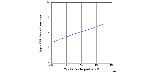
| ITRIP | TRIP source current | VTRIPx = 0.1 V, TA = 25°C | 8.5 | 10 | 11.5 | μA |
| TCITRIP | ITRIP temperature coefficient | On the basis of 25°C(1) | 4000 | ppm/°C | ||
| VOCLoff | OCP compensation offset | (VTRIPx-GND-VPGNDx-SWx) voltage, VTRIPx-GND = 60 mV, TA = 25°C |
–15 | 0 | 15 | mV |
| (VTRIPx-GND-VPGNDx-SWx) voltage, VTRIPx-GND = 60 mV |
–20 | 20 | ||||
| VRtrip | Current limit threshold setting range | VTRIPx-GND voltage | 30 | 300 | mV | |
| OUTPUT UNDERVOLTAGE AND OVERVOLTAGE PROTECTION | ||||||
| VOVP | Output OVP trip threshold | OVP detect | 110% | 115% | 120% | |
| VUVP | Output UVP trip threshold | UVP detect | 65% | 70% | 75% | |
| Hysteresis (recovery < 20 μs) | 10% | |||||
| THERMAL SHUTDOWN | ||||||
| TSDN | Thermal shutdown threshold | Shutdown temperature(1) | 150 | °C | ||
| Hysteresis(1) | 20 | |||||
(1) Ensured by design. Not production tested.
7.6 Timing Requirements
| TEST CONDITIONS | MIN | TYP | MAX | UNIT | ||
|---|---|---|---|---|---|---|
| OUTPUT: N-CHANNEL MOSFET GATE DRIVERS | ||||||
| tD | Dead time | DRVHx-low to DRVLx-on | 20 | 50 | 80 | ns |
| DRVLx-low to DRVHx-on | 20 | 40 | 80 | |||
| OUTPUT UNDERVOLTAGE AND OVERVOLTAGE PROTECTION | ||||||
| tOVPDEL | Output OVP prop delay time | 1.5 | μs | |||
| tUVPDEL | Output UVP delay time | 17 | 30 | 40 | μs | |
| tUVPEN | Output UVP enable delay time | UVP enable delay | 1.2 | 2 | 2.5 | ms |
7.7 Switching Characteristics
over operating free-air temperature range (unless otherwise noted)| PARAMETER | TEST CONDITIONS | MIN | TYP | MAX | UNIT | |
|---|---|---|---|---|---|---|
| ON-TIME TIMER CONTROL | ||||||
| tON1L | CH1 on time | SW1 = 12 V, VO1 = 1.8 V, TEST2 = 0 V | 490 | ns | ||
| tON2L | CH2 on time | SW2 = 12 V, VO2 = 1.8 V, TEST2 = 0 V | 390 | ns | ||
| tOFF1L | CH1 min off time | SW1 = 0.7 V, TA = 25°C, VFB1 = 0.7 V, TEST2 = 0 V | 285 | ns | ||
| tOFF2L | CH2 min off time | SW2 = 0.7 V, TA = 25°C, VFB2 = 0.7 V, TEST2 = 0 V | 285 | ns | ||
| tON1H | CH1 on time | SW1 = 12 V, VO1 = 1.8 V, TEST2 = V5FILT | 165 | ns | ||
| tON2H | CH2 on time | SW2 = 12 V, VO2 = 1.8 V, TEST2 = V5FILT | 140 | ns | ||
| tOFF1H | CH1 min off time | SW1 = 0.7 V, TA = 25°C, VFB1 = 0.7 V, TEST2 = V5FILT | 216 | ns | ||
| tOFF2H | CH2 min off time | SW2 = 0.7 V, TA = 25°C, VFB2 = 0.7 V, TEST2 = V5FILT | 216 | ns | ||
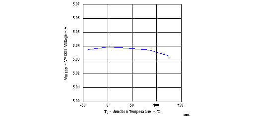
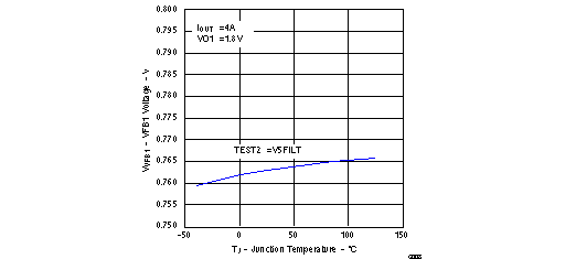
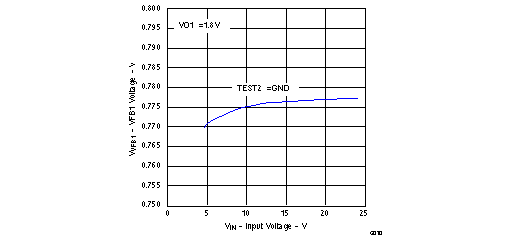
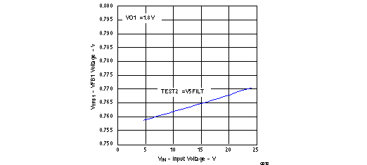
7.8 Typical Characteristics
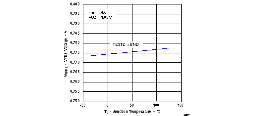
| CH2 = 1.05 V, IO = 4 A |
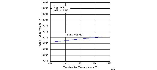
| CH2 = 1.05 V, IO = 4 A |
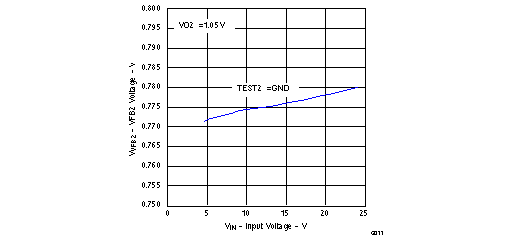
| CH2 = 1.05 V |
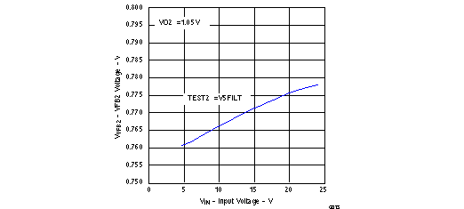
| CH2 = 1.05 V |
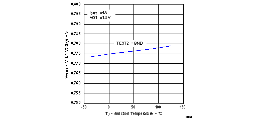
| CH1 = 1.8 V, IO = 4 A |
| CH1 = 1.8 V, IO = 4 A |
| CH1 = 1.8 V |
| CH1 = 1.8 V |