ZHCSL06D February 2008 – February 2020 TPS51200
PRODUCTION DATA.
- 1 特性
- 2 应用
- 3 说明
- 4 修订历史记录
- 5 Pin Configuration and Functions
- 6 Specifications
-
7 Detailed Description
- 7.1 Overview
- 7.2 Functional Block Diagram
- 7.3
Feature Description
- 7.3.1 Sink and Source Regulator (VO Pin)
- 7.3.2 Reference Input (REFIN Pin)
- 7.3.3 Reference Output (REFOUT Pin)
- 7.3.4 Soft-Start Sequencing
- 7.3.5 Enable Control (EN Pin)
- 7.3.6 Powergood Function (PGOOD Pin)
- 7.3.7 Current Protection (VO Pin)
- 7.3.8 UVLO Protection (VIN Pin)
- 7.3.9 Thermal Shutdown
- 7.3.10 Tracking Start-up and Shutdown
- 7.3.11 Output Tolerance Consideration for VTT DIMM Applications
- 7.3.12 REFOUT (VREF) Consideration for DDR2 Applications
- 7.4 Device Functional Modes
- 8 Application and Implementation
- 9 Power Supply Recommendations
- 10Layout
- 11器件和文档支持
- 12机械、封装和可订购信息
7.3.11 Output Tolerance Consideration for VTT DIMM Applications
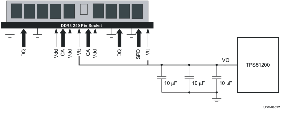
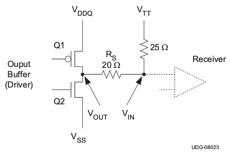
The TPS51200 is specifically designed to power up the memory termination rail (as shown in Figure 21). The DDR memory termination structure determines the main characteristics of the VTT rail, which is to be able to sink and source current while maintaining acceptable VTT tolerance. See Figure 22 for typical characteristics for a single memory cell.
 Figure 21. Typical Application Diagram for DDR3 VTT DIMM using TPS51200
  Figure 22. DDR Physical Signal System Bi-Directional SSTL Signaling
 In Figure 22, when Q1 is on and Q2 is off:
- Current flows from VDDQ via the termination resistor to VTT
- VTT sinks current
In Figure 22, when Q2 is on and Q1 is off:
- Current flows from VTT via the termination resistor to GND
- VTT sources current
Because VTT accuracy has a direct impact on the memory signal integrity, it is imperative to understand the tolerance requirement on VTT. Equation 1 applies to both DC and AC conditions and is based on JEDEC VTT specifications for DDR and DDR2 (JEDEC standard: DDR JESD8-9B May 2002; DDR2 JESD8-15A Sept 2003).
The specification itself indicates that VTT must keep track of VTTREF for proper signal conditioning.
The TPS51200 ensures the regulator output voltage to be as shown in Equation 2, which applies to both DC and AC conditions.
where
- –2 A < IVTT < 2 A
The regulator output voltage is measured at the regulator side, not the load side. The tolerance is applicable to DDR, DDR2, DDR3, DDR3L, Low Power DDR3, and DDR4 applications (see Table 1 for detailed information). To meet the stability requirement, a minimum output capacitance of 20 μF is needed. Considering the actual tolerance on the MLCC capacitors, three 10-μF ceramic capacitors sufficiently meet the VTT accuracy requirement.
Table 1. DDR, DDR2, DDR3 and LP DDR3 Termination Technology
| DDR | DDR2 | DR3 | LOW POWER DDR3 | |
|---|---|---|---|---|
| FSB Data Rates | 200, 266, 333, and 400 MHz | 400, 533, 677, and 800 MHz | 800, 1066, 1330, and 1600 MHz | |
| Termination | Motherboard termination to VTT for all signals | On-die termination for data group. VTT termination for address, command and control signals | On-die termination for data group. VTT termination for address, command and control signals | |
| Termination Current Demand | Maximum source/sink transient currents of up to 2.6 A to 2.9 A | Not as demanding | Not as demanding | |
| Only 34 signals (address, command, control) tied to VTT | Only 34 signals (address, command, control) tied to VTT | |||
| ODT handles data signals | ODT handles data signals | |||
| Less than 1-A of burst current | Less than 1-A of burst current | |||
| Voltage Level | 2.5-V Core and
I/O 1.25-V VTT |
1.8-V Core and
I/O 0.9-V VTT |
1.5-V Core and
I/O 0.75-V VTT |
1.2-V Core and
I/O 0.6-V VTT |
The TPS51200 uses transconductance (gM) to drive the LDO. The transconductance and output current of the device determine the voltage droop between the reference input and the output regulator. The typical transconductance level is 250 S at 2 A and changes with respect to the load in order to conserve the quiescent current (that is, the transconductance is very low at no load condition). The (gM) LDO regulator is a single pole system. Only the output capacitance determines the unity gain bandwidth for the voltage loop, as a result of the bandwidth nature of the transconductance (see Equation 3).

where
- ƒUGBW is the unity gain bandwidth
- gM is transconductance
- COUT is the output capacitance
Consider these two limitations to this type of regulator that come from the output bulk capacitor requirement. In order to maintain stability, the zero location contributed by the ESR of the output capacitors must be greater than the –3-dB point of the current loop. This constraint means that higher ESR capacitors should not be used in the design. In addition, the impedance characteristics of the ceramic capacitor should be well understood in order to prevent the gain peaking effect around the transconductance (gM) –3-dB point because of the large ESL, the output capacitor and parasitic inductance of the VO pin voltage trace.