ZHCSET1B December   2015  – March 2018 TPS4H000-Q1

PRODUCTION DATA.  

  1. 特性
  2. 应用
  3. 说明
    1.     Device Images
      1.      典型应用原理图
      2.      驱动具有可调节电流限制的电容性负载
  4. 修订历史记录
  5. Device Comparison Table
  6. Pin Configuration and Functions
    1.     Pin Functions
  7. Specifications
    1. 7.1 Absolute Maximum Ratings
    2. 7.2 ESD Ratings
    3. 7.3 Recommended Operating Conditions
    4. 7.4 Thermal Information
    5. 7.5 Electrical Characteristics
    6. 7.6 Switching Characteristics
    7. 7.7 Typical Characteristics
  8. Detailed Description
    1. 8.1 Overview
    2. 8.2 Functional Block Diagram
    3. 8.3 Feature Description
      1. 8.3.1 Pin Current and Voltage Conventions
      2. 8.3.2 Accurate Current Sense
      3. 8.3.3 Adjustable Current Limit
      4. 8.3.4 Inductive-Load Switching-Off Clamp
      5. 8.3.5 Fault Detection and Reporting
        1. 8.3.5.1 Diagnostic Enable Function
        2. 8.3.5.2 Multiplexing of Current Sense
        3. 8.3.5.3 Fault Table
        4. 8.3.5.4 STx and FAULT Reporting
      6. 8.3.6 Full Diagnostics
        1. 8.3.6.1 Short-to-GND and Overload Detection
        2. 8.3.6.2 Open-Load Detection
          1. 8.3.6.2.1 Channel On
          2. 8.3.6.2.2 Channel Off
        3. 8.3.6.3 Short-to-Battery Detection
        4. 8.3.6.4 Reverse Polarity Detection
        5. 8.3.6.5 Thermal Fault Detection
          1. 8.3.6.5.1 Thermal Shutdown
      7. 8.3.7 Full Protections
        1. 8.3.7.1 UVLO Protection
        2. 8.3.7.2 Loss-of-GND Protection
        3. 8.3.7.3 Protection for Loss of Power Supply
        4. 8.3.7.4 Reverse-Current Protection
        5. 8.3.7.5 MCU I/O Protection
    4. 8.4 Device Functional Modes
      1. 8.4.1 Working Modes
  9. Application and Implementation
    1. 9.1 Application Information
    2. 9.2 Typical Application
      1. 9.2.1 Design Requirements
      2. 9.2.2 Detailed Design Procedure
      3. 9.2.3 Application Curves
  10. 10Power Supply Recommendations
  11. 11Layout
    1. 11.1 Layout Guidelines
    2. 11.2 Layout Examples
      1. 11.2.1 Without a GND Network
      2. 11.2.2 With a GND Network
  12. 12器件和文档支持
    1. 12.1 接收文档更新通知
    2. 12.2 社区资源
    3. 12.3 商标
    4. 12.4 静电放电警告
    5. 12.5 Glossary
  13. 13机械、封装和可订购信息

封装选项

机械数据 (封装 | 引脚)
散热焊盘机械数据 (封装 | 引脚)
订购信息

Inductive-Load Switching-Off Clamp

When switching an inductive load off, the inductive reactance tends to pull the output voltage negative. Excessive negative voltage could cause the power FET to break down. To protect the power FET, an internal clamp between drain and source is implemented, namely VDS(clamp).

Equation 5. TPS4H000-Q1 eq05-Vds-clamp_SLVSCV8.gif

During the period of demagnetization (tdecay), the power FET is turned on for inductance-energy dissipation. The total energy is dissipated in the high-side switch. Total energy includes the energy of the power supply (E(VS)) and the energy of the load (E(load)). If resistance is in series with inductance, some of the load energy is dissipated on the resistance.

Equation 6. TPS4H000-Q1 eq06-Ehss_SLVSCV8.gif

When an inductive load switches off, E(HSS) causes high thermal stressing on the device.. The upper limit of the power dissipation depends on the device intrinsic capacity, ambient temperature, and board dissipation condition.
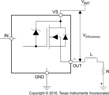
TPS4H000-Q1 D-to-S-clamp_SLVSCV8.gifFigure 27. Drain-to-Source Clamping Structure
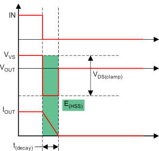
TPS4H000-Q1 load-switching_SLVSCV8.gifFigure 28. Inductive Load Switching-Off Diagram

From the perspective of the high-side switch, E(HSS) equals the integration value during the demagnetization period.
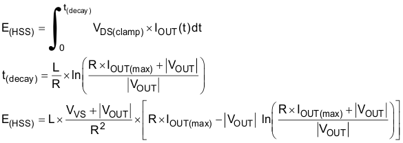
Equation 7. TPS4H000-Q1 eq07-Ehss_SLVSCV8.gif

When R approximately equals 0, E(HSD) can be given simply as:

Equation 8. TPS4H000-Q1 eq08-Ehss2_SLVSCV8.gif

Note that for PWM-controlled inductive loads, it is recommended to add the external free-wheeling circuitry shown in Figure 29 to protect the device from repetitive power stressing. TVS is used to achieve the fast decay. See Figure 29 for more details.
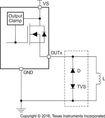
TPS4H000-Q1 prot_ext-circ_SLVSCV8.gifFigure 29. Protection With External Circuitry