ZHCSCO3A May 2014 – JULY 2014 TPS40428
PRODUCTION DATA.
- 1 特性
- 2 应用
- 3 说明
- 4 修订历史记录
- 5 Pin Configuration and Functions
- 6 Specifications
-
7 Detailed Description
- 7.1 Overview
- 7.2 Functional Block Diagram
- 7.3
Feature Description
- 7.3.1 Asynchronous Pulse Injection (API)
- 7.3.2 Adaptive Voltage Scaling (AVS)
- 7.3.3 Switching Frequency and Synchronization
- 7.3.4 Voltage Reference
- 7.3.5 Output Voltage and Remote Sensing Amplifier
- 7.3.6 Current Sensing and Temperature Sensing Modes
- 7.3.7 Current Sensing
- 7.3.8 Temperature Sensing
- 7.3.9 Current Sharing
- 7.3.10 Linear Regulators
- 7.3.11 Power Sequence Between TPS40428 Device and Power Stage
- 7.3.12 PWM Signal
- 7.3.13 Startup and Shutdown
- 7.3.14 Pre-Biased Output Start-up
- 7.3.15 PGOOD Indication
- 7.3.16 Overcurrent Protection
- 7.3.17 Output Overvoltage/Undervoltage Protection
- 7.3.18 Overtemperature Fault Protection
- 7.3.19 Input Undervoltage Lockout (UVLO)
- 7.3.20 Fault Communication
- 7.3.21 Fault Protection Summary
- 7.4 Device Functional Modes
- 7.5 Programming
- 7.6
Register Maps
- 7.6.1 PMBus General Description
- 7.6.2
PMBus Functionality
- 7.6.2.1 PMBus Address
- 7.6.2.2 PMBus Connections
- 7.6.2.3 PMBus Data Format
- 7.6.2.4 PMBus Output Voltage Adjustment
- 7.6.2.5 Reading the Output Current
- 7.6.2.6 Soft-Start Time
- 7.6.2.7 Turn-On/Turn-Off Delay and Sequencing
- 7.6.2.8
Supported PMBus Commands
- 7.6.2.8.1 PAGE (00h)
- 7.6.2.8.2 OPERATION (01h)
- 7.6.2.8.3 ON_OFF_CONFIG (02h)
- 7.6.2.8.4 CLEAR_FAULTS (03h)
- 7.6.2.8.5 WRITE_PROTECT (10h)
- 7.6.2.8.6 STORE_USER_ALL (15h)
- 7.6.2.8.7 RESTORE_USER_ALL (16h)
- 7.6.2.8.8 CAPABILITY (19h)
- 7.6.2.8.9 VOUT_MODE (20h)
- 7.6.2.8.10 VIN_ON (35h)
- 7.6.2.8.11 VIN_OFF (36h)
- 7.6.2.8.12 IOUT_CAL_GAIN (38h)
- 7.6.2.8.13 IOUT_CAL_OFFSET (39h)
- 7.6.2.8.14 IOUT_OC_FAULT_LIMIT (46h)
- 7.6.2.8.15 IOUT_OC_FAULT_RESPONSE (47h)
- 7.6.2.8.16 IOUT_OC_WARN_LIMIT (4Ah)
- 7.6.2.8.17 OT_FAULT_LIMIT (4Fh)
- 7.6.2.8.18 OT_WARN_LIMIT (51h)
- 7.6.2.8.19 TON_RISE (61h)
- 7.6.2.8.20 STATUS_BYTE (78h)
- 7.6.2.8.21 STATUS_WORD (79h)
- 7.6.2.8.22 STATUS_VOUT (7Ah)
- 7.6.2.8.23 STATUS_IOUT (7Bh)
- 7.6.2.8.24 STATUS_TEMPERATURE (7Dh)
- 7.6.2.8.25 STATUS_CML (7Eh)
- 7.6.2.8.26 STATUS_MFR_SPECIFIC (80h)
- 7.6.2.8.27 READ_VOUT (8Bh)
- 7.6.2.8.28 READ_IOUT (8Ch)
- 7.6.2.8.29 READ_TEMPERATURE_2 (8Eh)
- 7.6.2.8.30 PMBus_REVISION (98h)
- 7.6.2.8.31 MFR_SPECIFIC_00 (D0h)
- 7.6.2.8.32 MFR_SPECIFIC_04 (VREF_TRIM) (D4h)
- 7.6.2.8.33 MFR_SPECIFIC_05 (STEP_VREF_MARGIN_HIGH) (D5h)
- 7.6.2.8.34 MFR_SPECIFIC_06 (STEP_VREF_MARGIN_LOW) (D6h)
- 7.6.2.8.35 MFR_SPECIFIC_07 (PCT_VOUT_FAULT_PG_LIMIT) (D7h)
- 7.6.2.8.36 MFR_SPECIFIC_08 (SEQUENCE_TON_TOFF_DELAY) (D8h)
- 7.6.2.8.37 (E0h) MFR_SPECIFIC_16 (COMM_EEPROM_SPARE)
- 7.6.2.8.38 MFR_SPECIFIC_21 (OPTIONS) (E5h)
- 7.6.2.8.39 MFR_SPECIFIC_22 (PWM_OSC_SELECT) (E6h)
- 7.6.2.8.40 MFR_SPECIFIC_23 (MASK SMBALERT) (E7h)
- 7.6.2.8.41 MFR_SPECIFIC_25 (AVS_CONFIG) (E9h)
- 7.6.2.8.42 MFR_SPECIFIC_26 (AVS_ADDRESS) (EAh)
- 7.6.2.8.43 MFR_SPECIFIC_27 (AVS_DAC_DEFAULT) (EBh)
- 7.6.2.8.44 MFR_SPECIFIC_28 (AVS_CLAMP_HI) (ECh)
- 7.6.2.8.45 MFR_SPECIFIC_29 (AVS_CLAMP_LO) (EDh)
- 7.6.2.8.46 MFR_SPECIFIC_30 (TEMP_OFFSET) (EEh)
- 7.6.2.8.47 MFR_SPECIFIC_32 (API_OPTIONS) (F0h)
- 7.6.2.8.48 MFR_SPECIFIC_44 (DEVICE_CODE) (FCh)
-
8 Applications and Implementation
- 8.1 Application Information
- 8.2
Typical Application
- 8.2.1 Design Requirements
- 8.2.2
Detailed Design Procedure
- 8.2.2.1 Switching Frequency Selection
- 8.2.2.2 Inductor Selection
- 8.2.2.3 Output Capacitor Selection
- 8.2.2.4 Input Capacitor Selection
- 8.2.2.5 VDD, BP5, BP3 Bypass Capacitor
- 8.2.2.6 R-C Snubber
- 8.2.2.7 Current and Temperature Sensor
- 8.2.2.8 Power Sequence Between the TPS40428 Device and Power Stage
- 8.2.2.9 Output Voltage Setting and Frequency Compensation Selection
- 8.2.2.10 Key PMBus Parameter Selection
- 8.2.3 Application Curves
- 9 Power Supply Recommendations
- 10Layout
- 11器件和文档支持
- 12机械封装和可订购信息
11 器件和文档支持
11.1 开发支持
11.1.1 德州仪器 (TI) Fusion Digital Power Designer
德州仪器 (TI) Digital Power Designer 能够为 TPS40428 提供全面支持。 Fusion digital Power Designer 是一款图形用户界面 (GUI),可使用德州仪器 (TI) USB-to-GPIO 适配器通过 PMBus 来配置和监视 TPS40428 器件。
单击此链接下载德州仪器 (TI) Fusion Digital Power Designer 软件包。
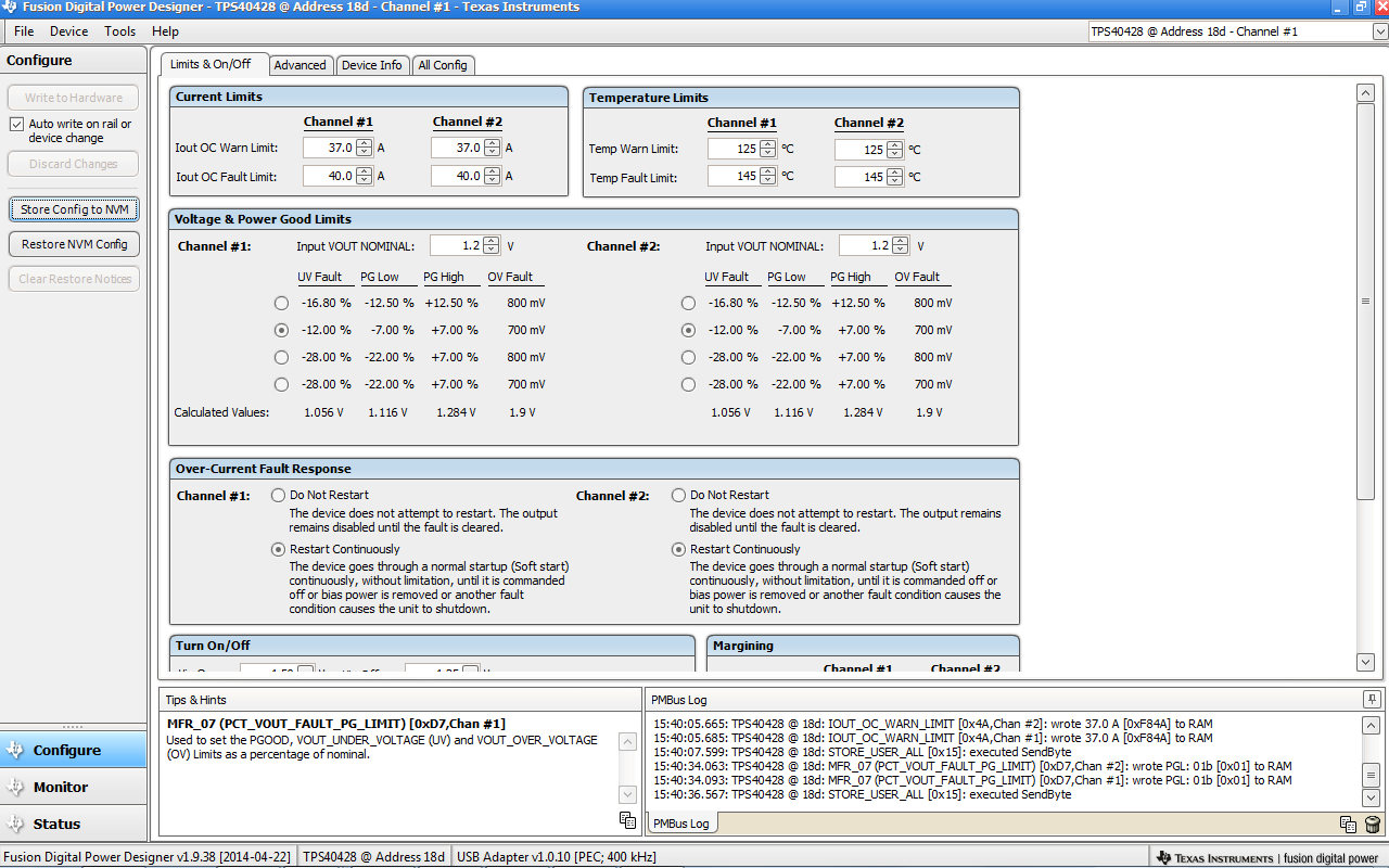 Figure 33. 使用 Fusion Digital Power Designer 进行器件配置
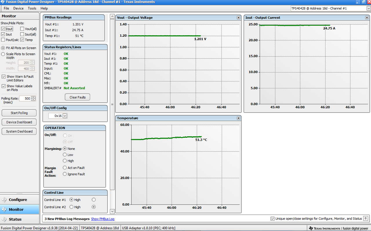 Figure 34. 使用 Fusion Digital Power Designer 进行器件监控
11.1.2 TPS40k 环路补偿工具
在双路输出应用中,TPS40428 器件是一款电压模式控制器;德州仪器 (TI) TPS40k 环路补偿工具可为其提供支持。 这款电子表格工具可用于计算频率补偿组件。
对于多相应用,将电流信息应用于控制环路可实现相位间的电流均流,TPS40428 器件此时不再是一个纯粹的电压模式控制器。 电子表格工具中计算得到的补偿组件值可用作起始点。
由于组件变化、PCB 寄生阻抗和布局影响,最好根据测量结果来优化补偿组件值。
11.2 Trademarks
All other trademarks are the property of their respective owners.
11.3 Electrostatic Discharge Caution

These devices have limited built-in ESD protection. The leads should be shorted together or the device placed in conductive foam during storage or handling to prevent electrostatic damage to the MOS gates.