ZHCS155C March 2011 – November 2023 TPS40170
PRODUCTION DATA
- 1
- 1 特性
- 2 应用
- 3 说明
- 4 Pin Configuration and Functions
- 5 Specifications
-
6 Detailed Description
- 6.1 Overview
- 6.2 Functional Block Diagram
- 6.3
Feature Description
- 6.3.1 LDO Linear Regulators and Enable
- 6.3.2 Input Undervoltage Lockout (UVLO)
- 6.3.3 Oscillator and Voltage Feed-Forward
- 6.3.4 Overcurrent Protection and Short-Circuit Protection (OCP and SCP)
- 6.3.5 Soft-Start and Fault-Logic
- 6.3.6 Overtemperature Fault
- 6.3.7 Tracking
- 6.3.8 Adaptive Drivers
- 6.3.9 Start-Up into Pre-Biased Output
- 6.3.10 Power Good (PGOOD)
- 6.3.11 PGND and AGND
- 6.4 Device Functional Modes
-
7 Application and Implementation
- 7.1 Application Information
- 7.2
Typical Application
- 7.2.1 Design Requirements
- 7.2.2
Detailed Design Procedure
- 7.2.2.1 Custom Design with WEBENCH® Tools
- 7.2.2.2 List of Materials
- 7.2.2.3 Select a Switching Frequency
- 7.2.2.4 Inductor Selection (L1)
- 7.2.2.5 Output Capacitor Selection (C9)
- 7.2.2.6 Peak Current Rating of Inductor
- 7.2.2.7 Input Capacitor Selection (C1, C6)
- 7.2.2.8 MOSFET Switch Selection (Q1, Q2)
- 7.2.2.9 Timing Resistor (R7)
- 7.2.2.10 UVLO Programming Resistors (R2, R6)
- 7.2.2.11 Boot-Strap Capacitor (C7)
- 7.2.2.12 VIN Bypass Capacitor (C18)
- 7.2.2.13 VBP Bypass Capacitor (C19)
- 7.2.2.14 VDD Bypass Capacitor (C16)
- 7.2.2.15 SS Timing Capacitor (C15)
- 7.2.2.16 ILIM Resistor (R9, C17)
- 7.2.2.17 SCP Multiplier Selection (R5)
- 7.2.2.18 Feedback Divider (R10, R11)
- 7.2.2.19 Compensation: (R4, R13, C13, C14, C21)
- 7.2.3 Application Curves
- 7.3 Power Supply Recommendations
- 7.4 Layout
- 8 Device and Documentation Support
- 9 Revision History
- 10Mechanical, Packaging, and Orderable Information
6.3.9 Start-Up into Pre-Biased Output
The TPS40170 contains a circuit to prevent current from being pulled out of the output during startup in case the output is pre-biased. When the soft-start commands a voltage higher than the pre-bias level (internal soft-start becomes greater than feedback voltage [VFB]), the controller slowly activates synchronous rectification by starting the first LDRV pulses with a narrow on-time (see Figure 6-16), where:
- VIN = 5 V
- VOUT = 3.3 V
- VPRE = 1.4 V
- fSW = 300 kHz
- L = 0.6 µH
It then increments the on-time on a cycle-by-cycle basis until it coincides with the time dictated by (1-D), where D is the duty cycle of the converter. This scheme prevents the initial sinking of the pre-bias output, and ensures that the output voltage (VOUT) starts and ramps up smoothly into regulation and the control loop is given time to transition from pre-biased startup to normal mode operation with minimal disturbance to the output voltage. The time from the start of switching until the low-side MOSFET is turned on for the full (1-D) interval is between approximately 20 and 40 clock cycles.
 Figure 6-16 Start-Up Switching Waveform during Pre-Biased Condition
 If the output is pre-biased to a voltage higher than the voltage commanded by the reference, then the PWM switching does not start.
When output is pre-biased at VPRE-BIAS, that voltage also applies to the SW node during start-up. When the pre-bias circuitry commands the first few high-side pulses before the first low-side pulse is initiated, the gate voltage for the high-side MOSFET is as described in Equation 18. Alternatively, If pre-bias level is high, it is possible that SCP can be tripped due to high turn-on resistance of the high-side MOSFET with low gate voltage. After tripped, the device resets and then attempts to re-start. The device can not be able to start up until output is discharged to a lower voltage level by either an active load or through feedback resistors.
In the case of a high pre-bias level, a low gate-threshold voltage rated device is recommended for the high-side MOSFET and increasing the SCP level also helps alleviate the problem.
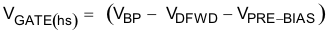
where
- VGATE(hs) is the gate voltage for the high-side MOSFET
- VBP is the BP regulator output
- VDFWD is bootstrap diode forward voltage