ZHCSM34M May 2004 – March 2023 TPS3808
PRODUCTION DATA
- 1 特性
- 2 应用
- 3 说明
- 4 Revision History
- 5 Device Voltage Thresholds
- 6 Pin Configuration and Functions
- 7 Specifications
- 8 Detailed Description
- 9 Application and Implementation
- 10Power Supply Recommendations
- 11Layout
- 12Device and Documentation Support
- 13Mechanical, Packaging, and Orderable Information
封装选项
机械数据 (封装 | 引脚)
散热焊盘机械数据 (封装 | 引脚)
- DRV|6
订购信息
8.3.3 Manual RESET ( MR) Input
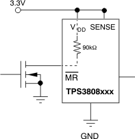
The manual reset ( MR) input allows a processor or other logic circuits to initiate a reset. A logic low (0.3 VDD) on MR causes RESET to assert. After MR returns to a logic high and SENSE is above its reset threshold, RESET is de-asserted after the user-defined reset delay expires. Note that MR is internally tied to VDD using a 90-kΩ resistor, so this pin can be left unconnected if MR is not used.
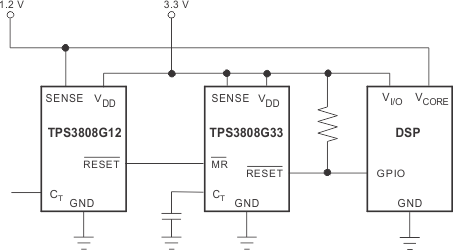
See Figure 8-3 for how MR can be used to monitor multiple system voltages. Note that if the logic signal driving MR does not go fully to VDD, there is some additional current draw into VDD as a result of the internal pullup resistor on MR. To minimize current draw, a logic-level FET can be used as illustrated in Figure 8-4.
 Figure 8-3 Using
MR to Monitor Multiple System Voltages
 Figure 8-4 Using an External MOSFET to Minimize IDD When
MR Signal Does Not Go to VDD